
Datasheet

IFX91041
Buck Regulator
Data Sheet 7 Rev. 1.1, 2011-07-08
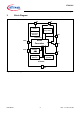
5 Buck Regulator
5.1 Description
The gate of the power switch is driven by the external capacitor connected to pin BDS (Buck Driver Supply) using
the bootstrap principle. An integrated under voltage lockout function supervising the ’bootstrap’ capacitor voltage
ensures that the device is always driven with a sufficient bootstrap voltage in order to prevent from extensive heat
up of the power transistor. An integrated charge pump supports the gate drive in case of low input supply voltage,
small differential voltage between input supply and output voltage at low current and during startup. In order to
minimize emission, the charge pump is switched off if the input voltage is sufficient for supplying the bootstrap.
The soft start function generates a defined ramp of the output voltage during the first 0.5 ms (typ.) after device
initialization. The device initialization is triggered either by the EN voltage level crossing the turn-on threshold,
rising supply voltage (during EN=H), and also when the device restarts a after thermal shutdown. The ramp starts
after the BDS external capacitor is charged.
The regulation scheme uses a voltage controlled pulse width modulation with feed forward path (the feed forward
operates for supply voltages from 8.0V to 36V) which provides a fast line transient reaction.
In order to maintain the output voltage regulation even under low duty cycle conditions (light load conditions down
to ICC=0mA, high input voltage) a pulse skipping operation mode is implemented. Pulse skipping is also used for
operation with low supply voltages, related to high duty cycles >92%
In case of a lost connection to the pin FB , an internal pull-up current prevents from a uncontrolled rise of the output
voltage (version IFX91041EJV only).
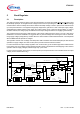
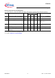
Figure 3 Block Diagram Buck Regulator
t
f
t
r
t
r
Schmitt-Trigger 1
V
high
V
low
t
Ramp
SYNC
&
&
R
Q
S
OFF
when H
Q
Clock
>1
_
Error -FF
L when
T
j
> 175 °C
Error
Amp.
FB
COMP
Error -Signal
Error -Ramp
PWM
Comp.
H when
Error-Signal <
Error -Ramp
Output Stage
OFF when H
NOR1
L when Overcurrent
&
NAND 2
&
&
R
Q
S
H =
OFF
Q
PWM-FF
1
INV
H =
ON
Gate
Driver
Gate Driver
Supply
Power
D-MOS
BUO
BDS
OC
Comp.
=
V
S
BDS
UV Comp.
H when
UV at
V
BDS
Charge
Pump
=
t
r
t
r
t
f
Oscillator
V
max
V
min
t
Soft start
Ramp
Generator
V
Ref
0.6 V
=
ΔV=k
X
V
S
Feedforward
L when
Output
overvoltage