
Datasheet

Data Sheet 6 Rev. 1.1, 2011-07-08
IFX91041
General Product Characteristics
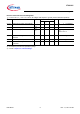
4.2 Functional Range
Note: Within the functional range the IC operates as described in the circuit description. The electrical
characteristics are specified within the conditions given in the related electrical characteristics table.
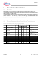
4.3 Thermal Resistance
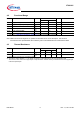
Pos. Parameter Symbol Limit Values Unit Conditions
Min. Max.
4.2.1 Supply Voltage
V
S
4.75 45 V –
4.2.2 Output Voltage adjust range
V
CC
0.60 16 V IFX91041EJV
4.2.3 Buck inductor
L
BU
18 56 µH –
4.2.4 Buck capacitor
C
BU1
33 120 µF –
4.2.5 Buck capacitor ESR
ESR
BU1
–0.3Ω –
1)
1) See section ““Application Information” on Page 12” for loop compensation requirements.
4.2.6 Junction Temperature T
j
-40 125 °C–
Pos. Parameter Symbol Limit Values Unit Conditions
Min. Typ. Max.
4.3.1 Junction to Case
1)
1) Not subject to production test, specified by design.
R
thJC
––12K/W–
4.3.2 Junction to ambient
1)
R
thJA
–52–K/W
2)
2) According to Jedec JESD52-1,-5,-7 at natural convection on 2s2p FR4 PCB for 1W power dissipation. PCB
76.2x114.3x1.5mm
3
with 2 inner copper layers of 70µm thickness. Thermal via array conected to the first inner copper layer
under the exposed pad.