
Datasheet

IFX91041
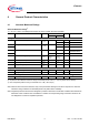
General Product Characteristics
Data Sheet 5 Rev. 1.1, 2011-07-08
4 General Product Characteristics
4.1 Absolute Maximum Ratings
Note: Stresses above the ones listed here may cause permanent damage to the device. Exposure to absolute
maximum rating conditions for extended periods may affect device reliability.
Note: Integrated protection functions are designed to prevent IC destruction under fault conditions described in the
data sheet. Fault conditions are considered as “outside” normal operating range. Protection functions are
not designed for continuous repetitive operation.
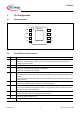
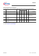
Absolute Maximum Ratings
1)
T
j
= -40 °C to +125°C; all voltages with respect to ground (unless otherwise specified)
1) Not subject to production test, specified by design.
Pos. Parameter Symbol Limit Values Unit Conditions
Min. Max.
Voltages
4.1.1 Synchronization Input
V
SYNC
-0.3 5.5 V –
6.2 V
t < 10s
2)
2) Exposure to those absolute maximum ratings for extended periods of time (t > 10s) may affect device reliability
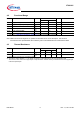
4.1.2 Compensation Input V
COMP
-0.3 5.5 V –
4.1.3 6.2 V
t < 10s
1)
4.1.4 Feedback Input V
FB
-0.3 10 V IFX91041EJV50;
IFX91041EJV33
4.1.5 -0.3 5.5 V IFX91041EJV
4.1.6 Buck Driver Supply Input
V
BDS
V
BUO
- 0.3
V
BUO
+ 5.5
V
4.1.7 Buck Switch Output
V
BUO
-2.0 V
VS
+ 0.3 V
4.1.8 Enable Input
V
EN
-40 45 V
4.1.9 Supply Voltage Input
V
VS
-0.3 45 V
Temperatures
4.1.10 Junction Temperature
T
j
-40 150 °C–
4.1.11 Storage Temperature
T
stg
-55 150 °C–
ESD Susceptibility
4.1.12 ESD Resistivity
V
ESD
-2 2 kV HBM
3)
3) ESD susceptibility HBM according to EIA/JESD 22-A 114B (1.5kΩ,100pF).