
Datasheet

Data Sheet 4 Rev. 1.1, 2011-07-08
IFX91041
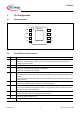
Pin Configuration
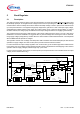
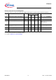
3 Pin Configuration
3.1 Pin Assignment
Figure 2 Pin Configuration
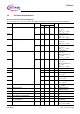
3.2 Pin Definitions and Functions
Pin Symbol Function
1SYNCSynchronization Input.
Connect to an external clock signal in order to synchronize/adjust the switching frequency.
If not used connect to GND.
2GNDGround.
3
COMP
Compensation Input.
Frequency compensation for regulation loop stability.
Connect to compensation RC-network.
4FB Feedback Input.
For the adjustable output voltage versions (IFX91041EJV) connect via voltage divider to output
capacitor.
For the fixed voltage version (IFX91041EJV50, IFX91041EJV33) connect this pin directly to the
output capacitor.
5BDS Buck Driver Supply Input.
Connect the bootstrap capacitor between this pin and pin BUO.
6BUO Buck Switch Output.
Source of the integrated power-DMOS transistor. Connect directly to the cathode of the catch
diode and the buck circuit inductance.
7EN Enable Input.
Active-high enable input with integrated pull down resistor.
8VS Supply Voltage Input.
Connect to supply voltage source.
Exposed Pad Connect to heatsink area and GND by low inductance wiring.
GND EN
COMP BUO
VS
5
6
4
3
2 7
1 8
FB
IFX91041
SYNC
BDS
S08_ PIN.vsd