
Datasheet


Data Sheet 14 Rev. 1.1, 2011-07-08
IFX91041
Application Information
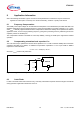
8.5 Adjustable Output Voltage Device
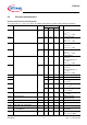
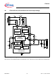
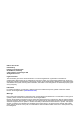
Figure 6 Application Diagram IFX91041EJV
Note: This is a very simplified example of an application circuit. The function must be verified in the real application
The output voltage of the IFX91041EJV can be programmed by a voltage divider connected to the feedback pin
FB. The divider cross current should be 300 µA at minimum, therefore the maximum
R
2
calculates:
R
2
≤ V
FB
/ I
R2
--> R
2
≤ 0.6V / 300 µA = 2 kΩ
For the desired output voltage level
V
CC
, R
1
calculates then (neglecting the small FB input current):
Add a 0.5 nF capacitor close to FB pin.
V
Batt
V
OUT
D
1
L
I
22…47µH
Ignition Key
Terminal 15
L
BU
C
BU1
D
BU
47µH
100µF
C
BU2
220nF
220nF
C
BOT
R
1
R
2
8
2
GND
Biasing &
Enable
Oscillator
7
4
Buck
Converter
6
FB
BUO
3
COMP
IFX91041EJV
1
SYNC
5
BDS
EN VS
Over
Temperature
Shutdown
Feedforward
Soft start ramp
generator
Bandgap
Reference
C
COMP
Charge Pump
R
COMP
C
FB
R
1
R
2
V
CC
V
FB
---------- 1–
⎝⎠
⎛⎞
.=