
Datasheet


Data Sheet 12 Rev. 1.1, 2011-07-08
IFX91041
Application Information
8 Application Information
Note: The following information is given as a hint for the implementation of the device only and shall not be
regarded as a description or warranty of a certain functionality, condition or quality of the device.
8.1 Frequency Compensation
The stability of the output voltage can be achieved with a simple RC connected between pin COMP and GND. The
standard configuration using the swiching frequency of the internal oscillator is a ceramic capacitor
C
COMP
=22nF
and
R
COMP
=22kΩ. By slight modifications to the compensation network the stability can be optimized for different
application needs, such as varying switching frequency (using the sychronizing function), different types of buck
capacitor (ceramic or tantalum) etc.
The compensation network is essential for control loop stability. Leaving pin COMP open might lead to instable
operation.
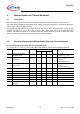
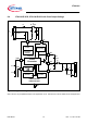
8.2 Compensating a tantalum buck capacitor C
BU1
The TLE control loop is optimized for ceramic buck capacitors C
BU
. In order to maintain stability also for tantalum
capacitors with ESR up to 300mΩ, an additional compensation capacitance
C
COMP2
at pin COMP to GND is
required. It’s value calculates:
C
COMP2
= C
BU
* ESR(C
BU
) / R
COMP
,
whereas
C
COMP2
needs to stay below 5nF.
Figure 4 High-ESR buck capacitor compensation
8.3 Catch Diode
In order to minimize losses and for fast recovery, a schottky catch diode is required. Disconnecting the catch diode
during operation might lead to destruction of the IC.
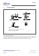
2
GND
3
COMP
IFX91041
C
COMP
R
COMP
C
COMP2
Application _C-COMP2.vsd