
Datasheet

IFX8117
General Product Characteristics
Data Sheet 9 Rev. 1.01, 2010-07-02
5.4 Electrical Characteristics
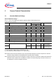
Electrical Characteristics Adjustable Version IFX8117MEV
0 °C ≤
T
j
≤ 125 °C, all voltages with respect to ground, positive current flowing into pin
(unless otherwise specified)
Pos. Parameter Symbol Limit Values Unit Conditions
Min. Typ. Max.
5.4.1 Reference Voltage
V
Ref
1.238 1.250 1.262 V I
Q
=10mA
V
I
- V
Q
=2V
T
J
=25°C
1.225 1.250 1.270 V 10 mA <
I
Q
<1A
1.4 V <
V
I
- V
Q
<10V
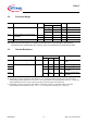
5.4.2 Line Regulation
1)
1) Measured at constant junction temperature
ΔV
Q,line
– 0.035 0.2 % of
V
Q
I
Q
=10mA
1.5 V <
V
I
- V
Q
< 13.75 V
5.4.3 Load Regulation
1)
ΔV
Q,load
– 0.2 0.4 % of
V
Q
V
I
- V
Q
=3V
10 mA < I
Q
<1A
5.4.4 Dropout Voltage
2)
V
dr
= V
I
- V
Q
2) Measured when the output voltage V
Q
has dropped 100mV from the nominal value obtained at V
I
= V
Q
+1.5V
V
dr
– 1.1 1.15 V
I
Q
= 100 mA
–1.151.2V
I
Q
= 500 mA
– 1.2 1.25 V
I
Q
= 1 A
5.4.5 Output Current Limitation I
Q,max
1.0 1.4 1.9 A V
I
- V
Q
= 5 V
T
J
=25°C
5.4.6 Minimum Load Current
3)
3) Minimum output current required to maintain regulation
I
Q,min
–0.45mAV
I
=15V
5.4.7 Thermal Regulation
ΔV
Q,power
–0.010.1% of
V
Q
per
1W
T
A
=25°C
30 ms pulse
5.4.8 Power Supply Ripple
Rejection
4)
4) Not subject to production test, specified by design
PSRR
60 75 – dB
V
I
- V
Q
= 3 V
f
ripple
= 120 Hz
V
ripple
= 1 V
pp
5.4.9 Adjust Pin Current
I
ADJ
10 30 50 µA
–
5.4.10 Adjust Pin Current Change
ΔI
ADJ
–0.25µA10mA<I
Q
<1A
1.4 V <
V
I
- V
Q
<10V
5.4.11 Temperature Stability
4)
ΔV
Q,temp
– 0.5 – % of
V
Q
–
5.4.12 Long Term Stability
4)
ΔV
Q,1000h
– 0.3 – % of
V
Q
T
A
= 125 °C
1000h
5.4.13 RMS Output Noise
4)
V
Q,RMS
– 0.003 – % of
V
Q
10 Hz < f <10kHz