
Datasheet

Data Sheet 8 Rev. 1.01, 2010-07-02
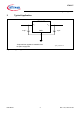
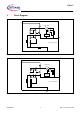
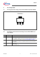
IFX8117
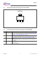
General Product Characteristics
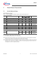
5.2 Functional Range
Note: Within the functional range the IC operates as described in the circuit description. The electrical
characteristics are specified within the conditions given in the related electrical characteristics table.
5.3 Thermal Resistance
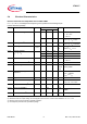
Pos. Parameter Symbol Limit Values Unit Conditions
Min. Max.
5.2.1 Input Voltage
V
I
V
Q
+ V
DR
15 V IFX8117MEV
4.55 15 V IFX8117MEV33
6.25 15 V IFX8117MEV50
5.2.2 Output Capacitor’s Requirements
for Stability
C
Q
10 – µF –
ESR(C
Q
)0.5 5 Ω –
5.2.3 Junction Temperature
T
j
0125°C–
Pos. Parameter Symbol Limit Values Unit Conditions
Min. Typ. Max.
5.3.1 Junction to Soldering Point
1)
1) not subject to production test, specified by design
R
thSP
– 15 – K/W measured to Pin 4
(Tab)
5.3.2 Junction to Ambient
1)
R
thJA
–51–K/W
2)
2) Specified R
thJA
value is according to Jedec JESD51-2,-5,-7 at natural convection on FR4 2s2p board; The Product
(Chip+Package) was simulated on a 76.2 x 114.3 x 1.5 mm board with 2 inner copper layers (2 x 70µm Cu, 2 x 35µm Cu).
Where applicable a thermal via array under the heat slug contacted the first inner copper layer.
5.3.3 – 146 – K/W Footprint only
3)
3) Specified R
thJA
value is according to Jedec JESD 51-3 at natural convection on FR4 1s0p board; The Product
(Chip+Package) was simulated on a 76.2 × 114.3 × 1.5 mm
3
board with 1 copper layer (1 x 70µm Cu).
5.3.4 – 75 – K/W 300mm
2
heatsink area
on PCB
3)
5.3.5 – 63 – K/W 600mm
2
heatsink area
on PCB
3)