
Datasheet

IFX8117
Pin Configuration
Data Sheet 5 Rev. 1.01, 2010-07-02
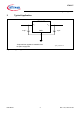
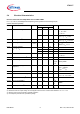
4 Pin Configuration
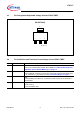
4.1 Pin Assignment Fixed Voltage Versions IFX8117MEV33 and IFX8117MEV50
Figure 4 Pin Assignment IFX8117MEV33 and IFX8117MEV50 (top view)
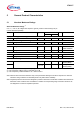
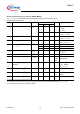
4.2 Pin Definitions and Functions Fixed Voltage Versions IFX8117MEV33 and
IFX8117MEV50
PG-SOT223-4
AEP02868_1117_01
123
4
QGND I
Q
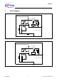
Pin Symbol Function
1GND Ground
2Q Output
block to GND with a capacitor close to the IC terminals, respecting the values given
for its capacitance C
Q
and ESR in the table “Functional Range” on Page 8
3
I
Input
for compensating line influences, a capacitor to GND close to the IC terminals is
recommended
4 (Tab) Q Output
connect to pin 2;
connect to heatsink area