
Datasheet

AEP02868_1117_02
123
4
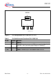
QADJ I
Q
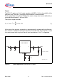
SOT223
Data Sheet 4 Rev. 1.0, 2011-02-24
IFX 1117
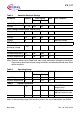
Figure 3 Pin Configuration IFX1117ME V (top view)
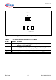
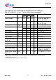
Table 2 Pin Definitions and Functions IFX1117ME V
Pin No. Symbol Function
1 ADJ Adjust; defines output voltage level by external voltage divider
between Q, ADJ and GND.
2 Q Output; Co
nnect output pin to GND via a capacitor C
Q
≥ 10 μF
with ESR ≤ 20 Ω (see also graph “Region of Stability”).
3 I Input
4 (TAB) Q Output; Connect to pin 2 and heatsink area on PCB