
Datasheet

Data Sheet 12 Rev. 1.0, 2009-05-14
IFX1050G
Application Information
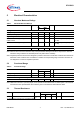
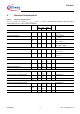
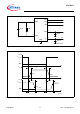
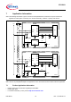
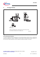
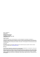
7 Application Information
Note: The following information is given as a hint for the implementation of the device only and shall not be
regarded as a description or warranty of a certain functionality, condition or quality of the device.
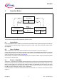
Figure 6 Mode State Diagram
Note: This is a very simplified example of an application circuit. The function must be verified in the real application.
7.1 Further Application Information
• Please contact us for information regarding the Pin FMEA.
• Existing App. Note
• For further information you may contact http://www.infineon.com/
ECU 1
ECU 1
µP
e. g. TLE4270
120
Ω
RM
5
INH
8
RxD
4
TxD
1
V
CC
3
CANH
CANL
7
6
100
nF
100
nF
+
V
Q
5 V
GND
GND
GND
V
I
22 µF
100
nF
+
22
µF
IFX1050
CAN
Bus
V
Bat
120 Ω
2
µP
e. g. TLE4270
RM
5
INH
8
RxD
4
TxD
1
V
CC
3
CANH
CANL
7
6
100
nF
100
nF
+
V
Q
5 V
GND
GND
GND
V
I
22 µF
100
nF
+
22
µF
IFX1050
2
ESD24VS2B
ESD24VS2B
1)
1)
1)
Optional