
Datasheet


Version 2.7 18 9 May 2012
CoolSET
®
-F3R
ICE3Bxx65J
Note: The trend of all the voltage levels in the Control Unit is the same regarding the deviation except V
VCCOVP
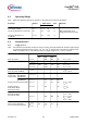
4.3.5 Current Limiting
4.3.6 CoolMOS
®
Section
Active Burst Mode Level for
Comparator C6b
V
FBC6b
2.88 3.00 3.12 V After Active Burst
Mode is entered
Overvoltage Detection Limit V
VCCOVP
19.5 20.5 21.5 V V
FB
= 5V, V
SoftS
= 3V
Thermal Shutdown
1)
T
jSD
130 140 150 °C
Spike Blanking t
Spike
- 8.0 - ms
1)
The parameter is not subject to production test - verified by design/characterization
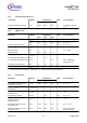
Parameter Symbol Limit Values Unit Test Condition
min. typ. max.
Peak Current Limitation (incl.
Propagation Delay Time)
(see Figure 11)
V
csth
1.01 1.06 1.11 V dV
sense
/ dt = 0.6V/ms
Peak Current Limitation during
Active Burst Mode
V
CS2
0.27 0.32 0.37 V
Leading Edge Blanking t
LEB
- 220 - ns V
SoftS
= 3.0V
CS Input Bias Current I
CSbias
-1.0 -0.2 0 µA V
CS
= 0V
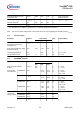
Parameter Symbol Limit Values Unit Test Condition
min. typ. max.
Drain Source Breakdown
Voltage
V
(BR)DSS
600
650
-
-
-
-
V
V
T
j
= 25°C
T
j
= 110°C
Drain Source
On-Resistance
ICE3B0365J R
DSon1
-
-
6.45
13.70
7.50
17.00
W
W
T
j
= 25°C
T
j
= 125°C
1)
at I
D
= 0.3A
ICE3B0565J R
DSon2
-
-
4.70
10.00
5.44
12.50
W
W
T
j
= 25°C
T
j
= 125°C
1)
at I
D
= 0.5A
ICE3B1565J R
DSon3
-
-
1.70
3.57
1.96
4.12
W
W
T
j
= 25°C
T
j
= 125°C
1)
at I
D
= 1.5A
ICE3B2065J R
DSon4
-
-
0.92
1.93
1.05
2.22
W
W
T
j
= 25°C
T
j
= 125°C
1)
at I
D
= 2.0A
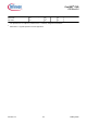
Effective output
capacitance,
energy related
ICE3B0365J C
o(er)1
- 3.65 - pF V
DS
= 0V to 480V
ICE3B0565J C
o(er)2
- 4.75 - pF
ICE3B1565J C
o(er)3
- 11.63 - pF
ICE3B2065J C
o(er)4
- 21 - pF