
Datasheet
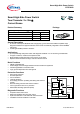

Data Sheet 8 V1.0, 2007-05-13
Smart High-Side Power Switch
BTS740S2
T
ru
th
T
a
bl
e
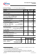
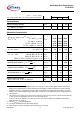
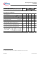
Input 1 Output 1 Status 1
Current
Sense 1
Input 2 Output 2 Status 2
Current
Sense 2
level level level I
IS
Normal
operation
L
H
L
H
H
L
0
nominal
Current-
limitation
L
H
L
H
H
H
0
0
Short circuit to
GND
L
H
L
L
21
)
H
H
0
0
Over-
temperature
L
H
L
L
H
H
0
0
Short circuit to
V
bb
L
H
H
H
L
22)
L
0
<nominal
23)
Open load L
H
L
24
)
H
H (L
25)
)
L
0
0
Undervoltage L
H
L
L
H
L
0
0
Overvoltage L
H
L
L
H
L
0
0
Negative output
voltage clamp
L L H 0
L = "Low" Level X = don't care Z = high impedance, potential depends on external circuit
H = "High" Level Status signal after the time delay shown in the diagrams (see fig 5. page 13)
Parallel switching of channel 1 and 2 is possible by connecting the inputs and outputs in parallel. The status
outputs ST1 and ST2 have to be configured as a 'Wired OR' function with a single pull-up resistor. The current
sense outputs IS1 and IS2 have to be connected with a single pull-down resistor.
Terms
352)(7
9
,6
67
*1'
EE
9
67
9
,1
,
67
,
,1
9
EE
,
EE
,
*1'
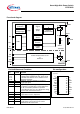
/HDGIUDPH
,1
9
,6
,
,6
9
287
9
21
,
/
287
5
*1'
&KLS
352)(7
9
,6
67
*1'
EE
9
67
9
,1
,
67
,
,1
,
*1'
/HDGIUDPH
,1
9
,6
,
,6
9
287
9
21
287
,
/
5
*1'
&KLS
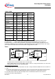
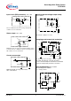
Leadframe (V
bb
) is connected to pin 1,10,11,12,15,16,19,20
External R
GND
optional; two resistors R
GND1
, R
GND2
= 150 Ω or a single resistor R
GND
=75 Ω for reverse
battery protection up to the max. operating voltage.
21)
The voltage drop over the power transistor is
V
bb
-
V
OUT
> 3V typ. Under this condition the sense current
I
IS
is
zero
22)
An external short of output to V
bb
, in the off state, causes an internal current from output to ground. If R
GND
is used, an offset voltage at the GND and ST pins will occur and the V
ST low
signal may be errorious.
23)
Low ohmic short to
V
bb
may reduce the output current
I
L
and therefore also the sense current
I
IS
.
24)
Power Transistor off, high impedance