
Datasheet

Data Sheet 7 V1.0, 2007-05-13
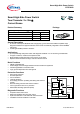
Smart High-Side Power Switch
BTS740S2
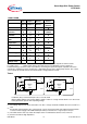
Parameter and Conditions,
each of the two channels
Symbol Values Unit
at Tj = -40...+150°C,
V
bb
= 12 V unless otherwise specified
min typ max
Input and Status Feedback
20)
Input resistance
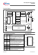
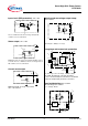
(see circuit page 9)
R
I
3.0 4.5 7.0 kΩ
Input turn-on threshold voltage
V
IN(T+)
-- -- 3.5 V
Input turn-off threshold voltage
V
IN(T-)
1.5 -- -- V
Input threshold hysteresis ∆
V
IN(T)
-- 0.5 -- V
Off state input current
V
IN
= 0.4 V:
I
IN(off)
1 -- 50 µA
On state input current
V
IN
= 5 V:
I
IN(on)
20 50 90 µA
Delay time for status with open load
after Input neg. slope
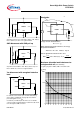
(see diagram page 13)
t
d(ST OL3)
-- 400 -- µs
Status delay after positive input slope
(not subject to production test, specified by design)
t
don(ST)
-- 13 --
µs
Status delay after negative input slope
(not subject to production test, specified by design)
t
doff(ST)
-- 1 --
µs
Status output (open drain)
Zener limit voltage
T
j
=-40...+150°C,
I
ST
= +1.6 mA:
ST low voltage
T
j
=-40...+25°C,
I
ST
= +1.6 mA:
T
j
= +150°C,
I
ST
= +1.6 mA:
V
ST(high)
V
ST(low)
5.4
--
--
6.1
--
--
6.9
0.4
0.7
V
Status leakage current,
V
ST
= 5 V,
T
j
=25 ... +150°C:
I
ST(high)
-- -- 2 µA
20)
If ground resistors R
GND
are used, add the voltage drop across these resistors.