
Datasheet

Data Sheet 6 V1.0, 2007-05-13
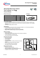
Smart High-Side Power Switch
BTS740S2
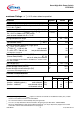
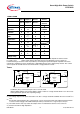
Parameter
and
Conditions
,
eac
h
o
f
th
e
t
wo c
h
anne
l
s
Symbol
Values
Unit
at Tj = -40...+150°C,
V
bb
= 12 V unless otherwise specified
min typ max
Reverse Battery
Reverse battery voltage
15
)
-
V
bb
-- -- 32 V
Drain-source diode voltage
(V
out
> V
bb
)
I
L
= - 4.0 A,
T
j
= +150°C
-
V
ON
-- 600 -- mV
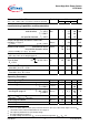
Diagnostic Characteristics
Current sense ratio
16)
, static on-condition,
V
IS
= 0...5 V,
V
bb(on)
= 6.5
17)
...27V,
k
ILIS
=
I
L
/
I
IS
T
j
= -40°C,
I
L
= 5 A:
k
ILIS
4350 4800 5800
T
j
= -40°C,
I
L
= 0.5 A: 3100 4800 7800
T
j
= 25...+150°C,
I
L
= 5 A:
T
j
= 25...+150°C,
I
L
= 0.5 A:
4350
3800
4800
4800
5350
6300
Current sense output voltage limitation
T
j
= -40 ...+150°C
I
IS
= 0,
I
L
= 5 A:
V
IS(lim)
5.4 6.1 6.9 V
Current sense leakage/offset current
T
j
= -40 ...+150°C
V
IN
=0,
V
IS
= 0,
I
L
= 0:
I
IS(LL)
0--1
µA
V
IN
=5 V,
V
IS
= 0,
I
L
= 0:
I
IS(LH)
0 -- 15
V
IN
=5 V,
V
IS
= 0,
V
OUT
= 0
(short circuit)
I
IS(SH)
18
)
0 -- 10
Current sense settling time to
I
IS static
±10% after
positive input slope
18)
,
I
L
= 0 5 A
t
son(IS)
-- -- 300
µs
Current sense settling time to 10% of
I
IS
static after
negative input slope
18)
,
I
L
= 5 0 A
t
soff(IS)
-- 30 100
µs
Current sense rise time (60% to 90%) after change
of load current
18)
I
L
= 2.5 5 A
t
slc(IS)
-- 10 --
µs
Open load detection voltage
19
)
(off-condition)
V
OUT(OL)
2 3 4 V
Internal output pull down
(
pin 17,18 to 2 resp. 13,14 to 6),
V
OUT
=5 V
R
O
5 15 40 kΩ
15)
Requires a 150 Ω resistor in GND connection. The reverse load current through the intrinsic drain-source
diode has to be limited by the connected load. Power dissipation is higher compared to normal operating
conditions due to the voltage drop across the drain-source diode. The temperature protection is not active
during reverse current operation! Input and Status currents have to be limited (see max. ratings page 3 and
circuit page 9).
16)
This range for the current sense ratio refers to all devices. The accuracy of the
k
ILIS
can be raised at least by
a factor of two by matching the value of
k
ILIS
for every single device.
In the case of current limitation the sense current
I
IS
is zero and the diagnostic feedback potential
V
ST
is
High. See figure 2c, page 12.
17)
Valid if
V
bb(u rst)
was exceeded before.
18)
not subject to production test, specified by design
19)
External pull up resistor required for open load detection in off state