
Datasheet
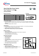
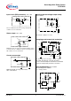

Data Sheet 4 V1.0, 2007-05-13
Smart High-Side Power Switch
BTS740S2
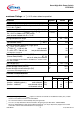
Parameter and Conditions, each of the two channels Symbol Values Unit
at Tj = -40...+150°C,
V
bb
= 12 V unless otherwise specified
min typ max
Load Switching Capabilities and Characteristics
On-state resistance (V
bb
to OUT);
I
L
= 5 A
each channel,
T
j
= 25°C:
T
j
= 150°C:
two parallel channels,
T
j
= 25°C:
R
ON
--
27
54
14
30
60
15
mΩ
Output voltage drop limitation at small load
currents,
see page 14
I
L
= 0.5 A
T
j
=-40...+150°C:
V
ON(NL)
-- 50 -- mV
Nominal load current one channel active:
two parallel channels active:
Device on PCB
6)
,
T
a
= 85°C,
T
j
≤ 150°C
I
L(NOM)
4.9
7.8
5.5
8.5
-- A
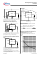
Output current while GND disconnected or pulled up
7)
;
V
bb
= 30 V,
V
IN
= 0, see diagram page 10
I
L(GNDhigh)
-- -- 8 mA
Turn-on time
8)
IN
to 90%
V
OUT
:
Turn-off time IN
to 10%
V
OUT
:
R
L
=12Ω
t
on
t
off
25
25
70
80
150
200
µs
Slew rate on
8)
10 to 30%
V
OUT
,
R
L
=12Ω:
d
V
/dt
on
0.1 -- 1 V/µs
Slew rate off
8)
70 to 40%
V
OUT
,
R
L
=12Ω:
-d
V
/dt
off
0.1 -- 1 V/µs
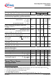
Operating Parameters
Operating voltage
9
)
V
bb(on)
5.0 -- 34 V
Undervoltage shutdown
V
bb(under)
3.2 -- 5.0 V
Undervoltage restart
T
j
=-40...+25°C:
T
j
=+150°C:
V
bb(u rst)
-- 4.5 5.5
6.0
V
Undervoltage restart of charge pump
see diagram page 13
T
j
=-40...+25°C:
T
j
=150°C:
V
bb(ucp)
--
--
4.7
--
6.5
7.0
V
Undervoltage hysteresis
∆
V
bb(under)
=
V
bb(u rst)
-
V
bb(under)
∆
V
bb(under)
-- 0.5 -- V
Overvoltage shutdown
V
bb(over)
34 -- 43 V
Overvoltage restart
V
bb(o rst)
33 -- -- V
6
)
Device on 50mm*50mm*1.5mm epoxy PCB FR4 with 6cm
2
(one layer, 70µm thick) copper area for V
bb
connection. PCB is vertical without blown air. See page 15
7
)
not subject to production test, specified by design
8
)
See timing diagram on page 11.
9)
At supply voltage increase up to
V
bb
= 4.7 V typ without charge pump,
V
OUT
≈
V
bb
- 2 V