
Datasheet

Data Sheet 2 V1.0, 2007-05-13
Smart High-Side Power Switch
BTS740S2
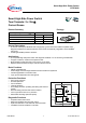
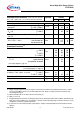
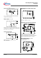
)XQFWLRQDOGLDJUDP
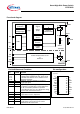
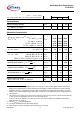
Pin Definitions and Functions
Pin Symbol Function
1,10,
11,12,
15,16,
19,20
V
bb
Positive power supply voltage. Design the
wiring for the simultaneous max. short circuit
currents from channel 1 to 2 and also for low
thermal resistance
3 IN1 Input 1,2, activates channel 1,2 in case of
7 IN2 logic high signal
17,18 OUT1 Output 1,2, protected high-side power output
13,14 OUT2 of channel 1,2. Both pins of each output have
to be connected in parallel for operation
according ths spec (e.g. k
ilis
). Design the wiring
for the max. short circuit current
4 ST1 Diagnostic feedback 1,2 of channel 1,2,
8 ST2 open drain, invers to input level
2 GND1 Ground 1 of chip 1 (channel 1)
6 GND2 Ground 2 of chip 2 (channel 2)
5 IS1
9 IS2
Sense current output 1,2; proportional to the
load current, zero in the case of current
limitation of the load current
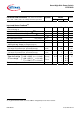
Pin configuration
(top view)
V
bb
1 • 20 V
bb
GND1 2 19 V
bb
IN1 3 18 OUT1
ST1 4 17 OUT1
IS1 5 16 V
bb
GND2 6 15 V
bb
IN2 7 14 OUT2
ST2 8 13 OUT2
IS2 9 12 V
bb
V
bb
10 11 V
bb
287
RYHUYROWDJH
S
URWHFWLRQ
ORJLF
LQWHUQDO
YROWD
J
HVX
SS
O
\
(6'
WHPSHUDWXUH
VHQVRU
FODPSIRU
LQGXFWLYHORDG
JDWH
FRQWURO
FKDUJH
SXPS
FXUUHQWOLPLW
2SHQORDG
GHWHFWLRQ
67
9%%
/2$'
,1
PROFET
*1'
Control and protection circuit
of
channel 2
,1
67
287
Channel 1
&XUUHQW
VHQVH
*1'
,6
,6
5
2
*1'