
Datasheet

Data Sheet 6 Rev. 1.3, 2010-03-16
Smart High-Side Power Switch
BTS721L1
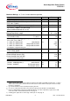
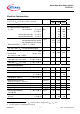
Parameter and Conditions,
each of the four channels
Symbol Values Unit
at Tj = 25 °C,
V
bb
= 12 V unless otherwise specified
min typ max
Leakage output current (included in
I
bb(off)
)
V
IN
=0
I
L(off)
-- -- 12 µA
Operating current
9)
,
V
IN
= 5V,
T
j
=-40...+150°C
I
GND
=
I
GND1/2
+
I
GND3/4
, one channel on:
four channels on:
I
GND
--
--
2
8
3
12
mA
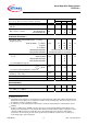
Protection Functions
10)
Initial peak short circuit current limit,
(see timing
diagrams
, page 13)
each channel,
T
j
=-40°C:
T
j
=25°C:
T
j
=+150°C:
I
L(SCp)
11
9
5
18
14
8
25
22
14
A
two parallel channels twice the current of one channel
four parallel channels four times the current of one channel
Repetitive short circuit current limit,
T
j
=
T
jt
each channel
two parallel channels
four parallel channels
(see timing diagrams, page 13)
I
L(SCr)
--
--
--
8
8
8
--
--
--
A
Initial short circuit shutdown time
T
j,start
=-40°C:
T
j,start
= 25°C:
(see page 12 and timing diagrams on page 13)
t
off(SC)
--
--
15
12
--
--
ms
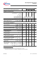
Output clamp (inductive load switch off)
11)
at V
ON(CL)
= V
bb
- V
OUT
V
ON(CL)
-- 47 -- V
Thermal overload trip temperature
T
jt
150 -- -- °C
Thermal hysteresis
∆
T
jt
-- 10 -- K
Reverse Battery
Reverse battery voltage
12
)
-
V
bb
-- -- 32 V
Drain-source diode voltage
(V
out
> V
bb
)
I
L
=-2.9 A,
T
j
=+150°C
-
V
ON
-- 610 -- mV
9)
Add
I
ST
, if
I
ST
> 0
10)
Integrated protection functions are designed to prevent IC destruction under fault conditions described in the
data sheet. Fault conditions are considered as "outside" normal operating range. Protection functions are not
designed for continuous repetitive operation.
11)
If channels are connected in parallel, output clamp is usually accomplished by the channel with the lowest
V
ON(CL)
12)
Requires a 150 Ω resistor in GND connection. The reverse load current through the intrinsic drain-source
diode has to be limited by the connected load. Note that the power dissipation is higher compared to normal
operating conditions due to the voltage drop across the intrinsic drain-source diode. The temperature
protection is not active during reverse current operation! Input and Status currents have to be limited (see
max. ratings page 3 and circuit page 8).