
Datasheet
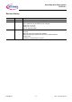

Data Sheet 13 Rev. 1.3, 2010-03-16
Smart High-Side Power Switch
BTS721L1
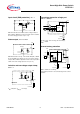
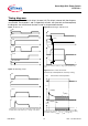
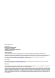
Figure 1a: V
bb
turn on:
,1
9
287
W
9
EE
67RSHQGUDLQ
,1
9
287
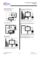
Figure 2a: Switching a lamp:
,1
67
287
/
W
9
,
The initial peak current should be limited by the lamp and not by
the initial short circuit current I
L(SCp)
= 14 A typ. of the device.
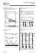
Figure 2b: Switching an inductive load
,1
67
/
W
9
,
287
W
G67
,
/2/
*) if the time constant of load is too large, open-load-status may
occur
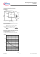
Figure 3a: Turn on into short circuit:
shut down by overtemperature, restart by cooling
RWKHUFKDQQHOQRUPDORSHUDWLRQ
W
,
67
,1
/
/6&U
,
,
/6&S
W
RII6&
Heating up of the chip may require several milliseconds, depending
on external conditions (t
off(SC)
vs. T
j,start
see page 12)
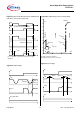
Timing diagrams
Timing diagrams are shown for chip 1 (channel 1/2). For chip 2 (channel 3/4) the diagrams
are valid too. The channels 1 and 2, respectively 3 and 4, are symmetric and consequently
the diagrams are valid for each channel as well as for permuted channels