
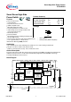
Datasheet
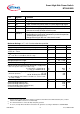
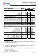

Thermal Characteristics
Parameter and Conditions Symbol Values Unit
min typ max
Thermal resistance chip - case:
R
thJC
-- -- 1.47
K/W
junction - ambient (free air):
R
thJA
-- -- 75
SMD version, device on PCB
4)
: -- 33 --
4)
Device on 50mm*50mm*1.5mm epoxy PCB FR4 with 6cm
2
(one layer, 70µm thick) copper area for V
bb
connection. PCB is vertical without blown air.
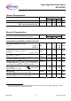
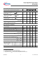
Electrical Characteristics
Parameter and Conditions Symbol Values Unit
at
T
j = 25 °C,
V
bb
= 12 V unless otherwise specified
min typ max
Load Switching Capabilities and Characteristics
On-state resistance
(pin 4 to 6&7)
I
L
= 5 A
T
j
=25 °C:
T
j
=150 °C:
R
ON
-- 27
54
30
60
mΩ
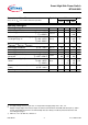
Output voltage drop limitation at small load
currents
(pin 4 to 6&7), see page 14
I
L
= 0.5 A
T
j
=-40...+150°C:
V
ON(NL)
-- 50 -- mV
Nominal load current, ISO Norm (pin 4 to 6&7)
V
ON
= 0.5 V,
T
C
= 85 °C
I
L(ISO)
11.4 12.6 -- A
Nominal load current, device on PCB
4)
T
A
= 85 °C,
T
j
≤ 150 °C
V
ON
≤ 0.5 V,
I
L(NOM)
4.0 4.5 -- A
Output current (pin 6&7) while GND disconnected
or GND pulled up,
V
bb
=30 V,
V
IN
= 0, see diagram page
9; not subject to production test, specified by design
I
L(GNDhigh)
-- -- 8 mA
Turn-on time IN to 90%
V
OUT
:
Turn-off time IN to 10%
V
OUT
:
R
L
= 12 Ω,
T
j
=-40...+150°C
t
on
t
off
25
25
70
80
150
200
µs
Slew rate on
10 to 30%
V
OUT
,
R
L
= 12 Ω,
T
j
=-40...+150°C
d
V
/dt
on
0.1 -- 1 V/µs
Slew rate off
70 to 40%
V
OUT
,
R
L
= 12 Ω,
T
j
=-40...+150°C
-d
V
/dt
off
0.1 -- 1 V/µs
Data Sheet 3 V1.1, 2008-19-08
Smart High-Side Power Switch
BTS640S2G