
Data Sheet
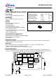


PROFET
®
BTS 6133D
Data Sheet Page 3 of 17 Rev. 1.0, 2007-02
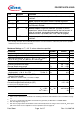
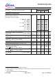
Thermal Characteristics
Parameter and Conditions Symbol Values Unit
min typ max
Thermal resistance chip - case:
R
thJC
-- -- 1.1
K/W
junction - ambient (free air): R
thJA
--
80 --
SMD version, device on PCB
5)
:
-- 45 55
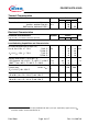
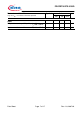
Electrical Characteristics
Parameter and Conditions Symbol Values Unit
at T
j
= 25, V
bb
= 12 V unless otherwise specified
min typ max
Load Switching Capabilities and Characteristics
On-state resistance (pin 3 to pin 1,5)
V
IN
= 0, V
bb
= 5.5V, I
L
= 7.5 A T
j
=25 °C:
T
j
=150 °C:
V
IN
= 0, V
bb
= 12V, I
L
= 7.5 A T
j
=25 °C:
T
j
=150 °C:
R
ON
--
--
--
--
10
18
8
14
14
26
10
18
mΩ
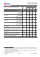
Nominal load current (Tab to pin 1,5)
ISO Proposal: V
ON
≤ 0.5 V, T
C
= 85°C, T
j
≤ 150°C
SMD
5)
: V
ON
≤ 0.5 V, T
A
= 85°C, T
j
≤ 150°C
I
L(ISO)
I
L(nom)
33
8
41
10
--
--
A
Turn-on time to 90% V
OUT
:
Turn-off time to 10% V
OUT
:
R
L
= 2.2 Ω, T
j
=-40...150 °C
t
on
t
off
--
--
250
250
500
500
µs
Slew rate on
25 to 50% V
OUT
, R
L
= 2.2 Ω, T
j
=-40...150 °C
dV /dt
on
-- 0.3 0.5 V/µs
Slew rate off
50 to 25% V
OUT
, R
L
= 2.2 Ω, T
j
=-40...150 °C
-dV/dt
off
-- 0.3 0.6 V/µs
5)
Device on 50mm*50mm*1.5mm epoxy PCB FR4 with 6cm
2
(one layer, 70µm thick) copper area for V
bb
connection. PCB is vertical without blown air.