
Datasheet

Datasheet 9 Rev. 1.1, 2008-11-04
Smart High-Side Power Switch
BTS5016SDA
Power Stages
5 Power Stages
The power stage is built by a N-channel vertical power MOSFET (DMOS) with charge pump.
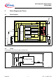
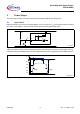
5.1 Input Circuit
Figure 4 shows the input circuit of the BTS5016SDA. The current source to V
bb
ensures that the device switches
off in case of open input pin. The zener diode protects the input circuit against ESD pulses.
Figure 4 Input Circuit
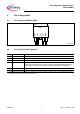
A high signal at the required external small signal transistor pulls the input pin to ground. A logic supply current
I
IN
is flowing and the power DMOS switches on with a dedicated slope, which is optimized in terms of EMC emission.
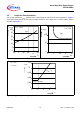
Figure 5 Switching a Load (resistive)
IN
R
bb
I
V
bb
Input.emf
V
Z,IN
V
IN
I
IN
V
bIN
V
OUT
t
SwitchOn.emf
t
I
IN
10%
25%
50%
90%
t
ON
t
OFF
(dV/dt)
ON
(d V/dt)
OFF