
Datasheet

Smart High-Side Power Switch
BTS5016SDA
Protection Functions
Datasheet 18 Rev. 1.1, 2008-11-04
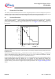
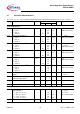
6.4 Overvoltage Protection
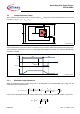
Beside the output clamp for the power stage as described in Section 5.3 there is a clamp mechanism
implemented for all logic pins. See Figure 15 for details.
Figure 15 Overvoltage Protection
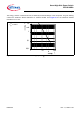
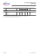
6.5 Loss of Ground Protection
In case of complete loss of the device ground connections the BTS5016SDA securely changes to or remains in
off state.
6.6 Loss of V
bb
Protection
In case of complete loss of V
bb
the BTS5016SDA remains in off state.
In case of loss of V
bb
connection with charged inductive loads a current path with load current capability has to be
provided, to demagnetize the charged inductances. It is recommended to use a diode, a Z-diode, or a varistor
(
V
ZL
+ V
D
<30V or V
Zb
+ V
D
<16V if R
IN
= 0). For higher clamp voltages currents through IN and IS have to be
limited to -120 mA. Please refer to Figure 16 for details.
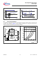
Figure 16 Loss of V
bb
OverVolt age .emf
IN
R
bb
V
bb
Logic
V
Z,IS
V
Z,IN
IS OUT
IN
R
bb
V
bb
Logic
IS
V
bb
R
IS
R
IN
V
D
V
ZL
inductive
LOAD
Vbb_disconnect _A. emf
IN
V
bb
Lo g ic
IS
V
bb
R
IS
R
IN
inductive
LOAD
V
D
V
Zb
Vbb_disconnect _B. emf
R
bb