
Datasheet

Datasheet 11 Rev. 1.1, 2008-11-04
Smart High-Side Power Switch
BTS5016SDA
Power Stages
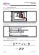
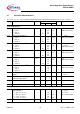
5.3 Output Inductive Clamp
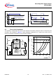
When switching off inductive loads, the output voltage V
OUT
drops below ground potential due to the involved
inductance ( -d
i
L
/dt =-v
L
/L ; -V
OUT
≅ -V
L
).
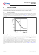
Figure 8 Output Clamp
To prevent destruction of the device, there is a voltage clamp mechanism implemented that keeps the voltage drop
across the device at a certain level (
V
ON(CL)
). See Figure 8 and Figure 9 for details. The maximum allowed load
inductance is limited.
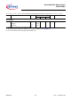
Figure 9 Switching an Inductance
5.3.1 Maximum Load Inductance
While de-energizing inductive loads, energy has to be dissipated in the BTS5016SDA. This energy can be
calculated via the following equation:
In the event of de-energizing very low ohmic inductances (
R
L
≈0) the following, simplified equation can be used:
Out put Clam p . emf
OUT
V
bb
VBB
L,
R
L
V
OUT
I
L
V
ON
V
OUT
InductiveLoad. emf
t
I
L
t
V
OUT(CL)
V
bb
ON OFF
V
ON(CL)
EV
ON CL()
V
bb
V
ON CL()
–
R
L
------------------------------------
ln⋅ 1
R
L
I
L
⋅
V
ON(CL)
V
bb
–
-----------------------------------+
I
L
+
L
R
L
----- -
⋅⋅=
E
1
2
-- -
LI
L
2
V
ON(CL)
V
ON(CL)
V
bb
–
-----------------------------------
⋅=