
Datasheet

Smart High-Side Power Switch
BTS50080-1TEB
Power Stages
Datasheet 10 Rev. 1.0, 2008-08-28
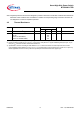
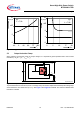
Figure 6 Typical On-State Resistance
5.3 Output Inductive Clamp
When switching off inductive loads, the output voltage V
OUT
drops below ground potential due to the involved
inductance ( -d
i
L
/dt =-v
L
/L ; -V
OUT
≅
-V
L
).
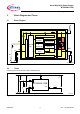
Figure 7 Output Clamp
To prevent destruction of the device, there is a voltage clamp mechanism implemented that keeps the voltage drop
across the device at a certain level (
V
ON(CL)
). See Figure 7 and Figure 8 for details. The maximum allowed load
inductance is limited.
ȍ
ȍ
Out put Clam p . emf
OUT
V
bb
VBB
L,
R
L
V
OUT
I
L
V
ON