
Datasheet
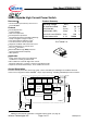

Data Sheet BTS50055-1TMC
Page 6 of 17 2010-April-27
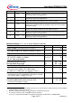
Parameter and Conditions Symbol Values Unit
at Tj = -40 ... +150 °C, V
bb
= 12 V unless otherwise specified
min typ max
Sense current saturation I
IS,lim
6.5 -- -- mA
Current sense leakage current I
IN
= 0:
V
IN
= 0, I
L
≤ 0:
I
IS(LL)
I
IS(LH)
--
--
--
2
0.5
--
µA
Current sense overvoltage protection
T
j
=-40°C:
I
bb
= 15 mA T
j
= 25...+150°C:
V
bIS(Z)
60
62
--
66
--
--
V
Current sense settling time
21
)
t
s(IS)
-- -- 500
µs
Input
Input and operating current (see diagram page 12)
IN grounded (V
IN
= 0)
I
IN(on)
-- 0.8 1.5 mA
Input current for turn-off
22
)
I
IN(off)
-- -- 80 µA
Truth Table
Input
current
Output Current
Sense
Remark
level
level I
IS
Normal
operation
L
H
L
H
0
nominal
=I
L
/ k
ilis
, up to I
IS
=I
IS,lim
Very high
load current
H H I
IS, lim
up to V
ON
=V
ON(Fold back)
I
IS
no longer proportional to I
L
Current-
limitation
H H 0
V
ON
> V
ON(Fold back)
Short circuit to
GND
L
H
L
L
0
0
Over-
temperature
L
H
L
L
0
0
Short circuit to
V
bb
L
H
H
H
0
<nominal
23
)
Open load L
H
Z
24
)
H
0
0
Negative output
voltage clamp
L L 0
Inverse load
current
L
H
H
H
0
0
L = "Low" Level
H = "High" Level
Overtemperature reset by cooling: T
j
< T
jt
(see diagram on page 14)
21
)
not subject to production test, specified by design
22
)
We recommend the resistance between IN and GND to be less than 0.5
kΩ for turn-on and more than
500
kΩ for turn-off. Consider that when the device is switched off (I
IN
= 0) the voltage between IN and GND
reaches almost V
bb
.
23
)
Low ohmic short to V
bb
may reduce the output current I
L
and can thus be detected via the sense current I
IS
.
24
)
Power Transistor "OFF", potential defined by external impedance.