
Datasheet
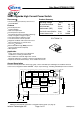

Data Sheet BTS50055-1TMC
Page 3 of 17 2010-April-27
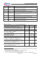
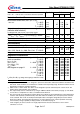
Thermal Characteristics
Parameter and Conditions Symbol Values Unit
min typ max
Thermal resistance chip - case:
R
thJC
7
)
-- -- 0.75
K/W
junction - ambient (free air): R
thJA
--
60 --
SMD version, device on PCB
8
)
:
33
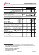
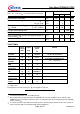
Electrical Characteristics
Parameter and Conditions Symbol Values Unit
at Tj = -40 ... +150 °C, V
bb
= 12 V unless otherwise specified
min typ max
Load Switching Capabilities and Characteristics
On-state resistance (Tab to pins 1,2,6,7)
V
IN
= 0, I
L
= 20 A T
j
= 25 °C:
T
j
= 150 °C:
V
IN
= 0, I
L
= 90 A T
j
= 150 °C:
V
bb
= 6V
9
)
, V
IN
= 0, I
L
= 20 A T
j
= 150 °C:
R
ON
--
--
4.4
7.9
--
10
6.0
10.5
10.7
17
mΩ
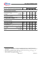
Nominal load current
10
)
, (Tab to pins 1,2,6,7)
ISO Proposal: V
ON
= 0.5 V,T
C
= 85°C,T
j
≤ 150°C
11
)
SMD
8)
: T
A
= 85 °C, T
j
≤ 150 °C V
ON
≤ 0.5 V
I
L(ISO)
I
L(NOM)
55
13.6
70
17
--
--
A
Maximum load current in resistive range
(Tab to pins 1,2,6,7) V
ON
= 1.8 V, T
c
= 25 °C:
see diagram on page 12 V
ON
= 1.8 V, T
c
= 150 °C:
I
L(Max)
250
150
--
--
--
--
A
Turn-on time
12
)
I
IN
to 90% V
OUT
:
Turn-off time I
IN
to 10% V
OUT
:
R
L
= 1 Ω , T
j
=-40...+150°C
t
on
t
off
130
90
230
130
450
210
µs
Slew rate on
12)
(10 to 30% V
OUT
)
R
L
= 1 Ω , T
J
= 25 °C
dV/dt
on
0.1 0.25 0.6 V/µs
Slew rate off
12)
(70 to 40% V
OUT
)
R
L
= 1 Ω , T
J
= 25 °C
-dV/dt
off
0.15 0.35 0.6 V/µs
7
)
Thermal resistance R
thCH
case to heatsink (about 0.5 ... 0.9 K/W with silicone paste) not included!
8
)
Device on 50mm*50mm*1.5mm epoxy PCB FR4 with 6cm
2
(one layer, 70µm thick) copper area for V
bb
connection. PCB is vertical without blown air.
9
)
Decrease of V
bb
below 10 V causes slowly a dynamic increase of R
ON
to a higher value of R
ON(Static)
. As
long as V
bIN
> V
bIN(u) max
, R
ON
increase is less than 10 % per second for T
J
< 85 °C.
10
)
not subject to production test, specified by design
11
)
T
J
is about 105°C under these conditions.
12
)
See timing diagram on page 13.