
Datasheet


Datasheet 8 Rev. 1.1, 2008-02-28
Smart Low Side Power Switch
HITFET - BTS3160D
General Product Characteristics
4 General Product Characteristics
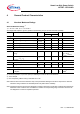
4.1 Absolute Maximum Ratings
T
j
= -40 °C to +150 °C; V
S
= 6 V to 30 V.
All voltages with respect to ground, positive current flowing into pin (unless otherwise specified)
Pos. Parameter Symbol Limit Values Unit Conditions
Min. Max.
Supply voltage V
S
-0.3 30 V –
Supply voltage during active clamping V
S(pulse)
-0.3 45 V
2) Not for DC operation, only for short pulse (i.e. loaddump) for a total of 100 h in full device life.
Drain voltage V
D
-0.3 40 V
3) Active clamped.
Drain voltage for short circuit protection V
D(SC)
0 30 V –
Logic input voltage V
IN
-0.3 5.3 V –
Unclamped single pulse inductive
energy
E
AS
0 0.3 J I
D
= 20 A;
V
bb
= 30 V
T
J(Start)
= 150°C
Load dump protection
V
LoadDump
= V
A
+ V
S
V
LD
0 45 V T
J
= 25°C
Junction Temperature T
j
-40 150 °C –
Storage Temperature T
stg
-55 150 °C –
ESD Resistivity
on all pins V
ESD
-4 4 kV
4) ESD susceptibility, HBM according to EIA/JESD 22-A114B
HBM
4)
3)
2)
Note: Stresses above the ones listed here may cause permanent damage to the device. Exposure to absolute
maximum rating conditions for extended periods may affect device reliability.
Note: Integrated protection functions are designed to prevent IC destruction under fault conditions described in the
data sheet. Fault conditions are considered as “outside” normal operating range. Protection functions are
not designed for continuous repetitive operation.
Absolute Maximum Ratings
1)
1) Not subject to production test, specified by design.
Voltages
4.1.1
4.1.2
4.1.3
4.1.4
4.1.5
Energies
4.1.6
4.1.7
Temperatures
4.1.8
4.1.9
ESD Susceptibility
4.1.10