
Datasheet


Datasheet 4 Rev. 1.1, 2008-02-28
Smart Low Side Power Switch
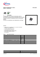
HITFET - BTS3160D
Overview
Digital Diagnostic
• Over temperature shutdown
• Over load shutdown
• Short circuit shutdown
Protection Functions
• Electrostatic discharge (ESD)
• Under voltage lock out
• Over temperature (shutdown with latch)
• Over voltage (active clamped)
Application
• Micro controller compatible low side power switch with digital feedback for 12V loads
• All types of resistive, inductive and capacitive loads
• Suitable for loads with high inrush current, such as lamps
• Also suitable for LEDs because of low leakage current
• Replaces electromechanical relays, fuses and discrete circuits
Description
The BTS3160D is a latching one channel low-side power switch in PG-TO-252-5-13 package providing embedded
protective functions. The power transistor is build by a N-channel vertical power MOSFET. The device is controlled
by a control chip in Smart Power Technology.
The device is able to switch all kind of resistive, inductive and capacitive loads. For lamp loads the lamp-inrush-
current, eight- to ten-times the nominal current, has to be considered. The maximal inrush current has to be below
the minimum short circuit shutdown current.
The ESD protection of the V
S
and IN/Fault pin is in relation to GND.
The BTS3160D is supplied by the V
S
Pin. This Pin can be connected to battery line. The supply voltage is
monitored by the under voltage lock out circuit. The Gate driving unit allows to operate the device in the low ohmic
range even with 3.3
V input signal. For PWM application the device offers smooth turn-on and off due to the
embedded edge shaping function, in order to reduce EMC noise.
The over voltage protection is for protection during load-dump or inductive turn off conditions. The power MOSFET
is limiting the drain-source voltage, if it gets too high. This function is available even without supply.
The over temperature protection is in order to save the device from overheating due to overload and bad cooling
conditions. In order to reduce the device stress the edge shaping is disabled during thermal shutdown. After
thermal shutdown the device stays off until the latch is reset by a IN-Low signal. For high dynamic overload
conditions such as short circuit the device will turn off if a certain load current is reached. The short circuit
shutdown is a latch function. The device will stay off until the latch is reset by IN-Low signal. In order to reduce the
device stress the edge shaping is disabled during short circuit turn off.