
Datasheet

Datasheet 21 Rev. 1.1, 2008-02-28
Smart Low Side Power Switch
HITFET - BTS3160D
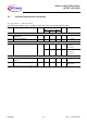
Power Stage
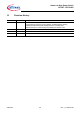
6.4.13 Slew rate between edge shaping |dI/dt|
fast
– – 0.3 A/µs
1)
R
L
= 2.2 Ω
V
bb
= V
S
= 13.5 V;
ohmic load
6.4.14 Fault signal delay t
dfault
– 4 10 µs
1)
Inverse Diode
6.4.15
Inverse Diode forward voltage V
D
-0.3 -1.0 -1.5 V I
D
= -12 A;
V
S
= 0 V;
V
IN
= 0.0 V
1) Not subject to production test.
2) Device on 50 mm × 50 mm × 1.5 mm epoxy PCB FR4 with 6 cm
2
(one layer, 70 µm thick) copper area for drain connection.
PCB mounted vertical without blown air.
V
S
= 6 V to 30 V, T
j
= -40 °C to +150 °C
All voltages with respect to ground, positive current flowing into pin (unless otherwise specified)
Pos. Parameter Symbol Limit Values Unit Conditions
Min. Typ. Max.