
Datasheet

Datasheet 17 Rev. 1.1, 2008-02-28
Smart Low Side Power Switch
HITFET - BTS3160D
Power Stage
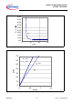
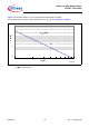
6.2 Output Timing and Slopes
A high signal on the input pin causes the power MOSFET to switch on with a dedicated slope which is optimized
for low EMC emission.
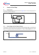
Figure 13 shows the timing definition.
IN
Low
High
t
on
t
off
t
V
D
V
bb
60 %
40 %
-dV
D
/ dt
on
dV
D
/ dt
off
OutputTiming.emf
t
t
ond
10 %
90 %
t
o ffd
Figure 13 Switching a resistive Load
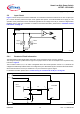
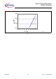
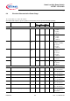
In order to minimize the emission during switching the BTS3160D limits the slopes during turn on- and off to slow
slew rate settings.
The definition is shown in Figure 14. For best performance of the edge shaping the supply pin V
S
should be connected to battery voltage. For supply voltages other than nominal battery the edge shaping can differ
from the values in the electrical characteristics table below.
IN
Low
High
t
I
D
20 %
|di/dt|slow
EdgeS haping.emf
t
80 %
100 %
|di/dt|slow
|di/dt|fast
Figure 14 Typical Slopes for resistive Loads