
Datasheet

Datasheet 12 Rev. 1.1, 2008-02-28
Smart Low Side Power Switch
HITFET - BTS3160D
Supply and Input Stage
5.2 Input Circuit
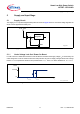
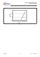
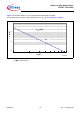
Figure 7 shows the input circuit of the BTS3160D. It’s ensured that the device switches off in case of open input
pin. A zener structure protects the input circuit against ESD pulses. As the BTS3160D has a supply pin, the
operation of the power MOS can be maintained regardless of the voltage on the IN pin, therefore a digital status
feedback down to logic low is realized. For readout of the fault information, please refer to
“Readout of Fault
Information” on Page 12
input.emf
GND
IN/Fault
1.0mA
:
3.0mA
20µA
:
100µA
Figure 7 Input Circuit
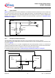
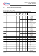
5.2.1 Readout of Fault Information
The BTS3160D provides digital status information via an increased current on the IN / Fault pin.
The voltage on this pin is pulled down to logic low if a proper resistor is used. An example for the required circuitry
is shown in Figure 8.
The increased current I
IN(fault)
is an order of magnitude above the normal operation current I
IN(nom)
therefore the
voltage at the IN/Fault pin will decrease. The voltage at the pin is determined by the current and the serial resistor.
We recommend 3k3 for a 3.3V µC and 5k6 for a 5V µC to achieve a logic low signal.
For detailed calculation please refer to “Dimensioning of serial Resistor at IN pin” on Page 26
IN/Fault
Fault_Readout.emf
BTS3160D
Micro
controller
V
CC
V
S
GND
GND
DO
DI
V
DI
I
DO
I
IN
R1
V
CC
GND
V
bb
Figure 8 Readout of Fault Information