
Datasheet

Datasheet 3 Rev. 1.3, 2006-12-22
Smart Low Side Power Switch
Power HITFET BTS 142D
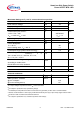
Electrical Characteristics
Parameter Symbol Values Unit
at T
j
= 25°C, unless otherwise specified min. typ. max.
Characteristics
Drain source clamp voltage
T
j
= - 40 ...+ 150 °C, I
D
= 10 mA
V
DS(AZ)
42 - 55 V
Off-state drain current
T
j
= -40...+85 °C, V
DS
= 32 V, V
IN
= 0 V
T
j
= 150 °C
I
DSS
-
-
1.5
10
8
20
µA
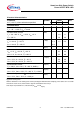
Input threshold voltage
I
D
= 2.4 mA, T
j
= 25 °C
I
D
= 2.4 mA, T
j
= 150 °C
V
IN(th)
1.3
0.8
1.7
-
2.2
-
V
On state input current I
IN
(
on
)
- 10 30 µA
On-state resistance
V
IN
= 5 V, I
D
= 4.6 A, T
j
= 25 °C
V
IN
= 5 V, I
D
= 4.6 A, T
j
= 150 °C
R
DS(on)
-
-
27
54
34
68
mW
On-state resistance
V
IN
= 10 V, I
D
= 4.6 A, T
j
= 25 °C
V
IN
= 10 V, I
D
= 4.6 A, T
j
= 150 °C
R
DS(on)
-
-
23
46
28
56
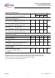
Nominal load current
5)
T
j
< 150°C, V
IN
= 10 V, T
A
= 85 °C, SMD
1)
I
D(Nom)
4.6 5.5 - A
Nominal load current
5)
V
IN
= 10 V, V
DS
= 0.5 V, T
C
= 85 °C, T
j
< 150°C
I
D(ISO)
12.6 15.3 -
Current limit (active if V
DS
>2.5 V)
2)
V
IN
= 10 V, V
DS
= 12 V, t
m
= 200 µs
I
D(lim)
30 45 55
1
@ 6 cm
2
cooling area
2
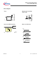
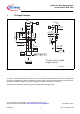
Device switched on into existing short circuit (see diagram Determination of I
D(lim)
). If the device is in on conditi
a
nd a short circuit occurs, these values might be exceeded for max. 50 µs.
5
not subject to production test, calculated by R
thJA
and R
ds(on)