
Datasheet

Datasheet 2 Rev. 1.3, 2006-12-22
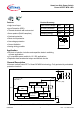
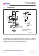
Smart Low Side Power Switch
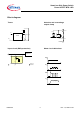
Power HITFET BTS 142D
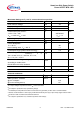
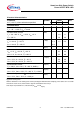
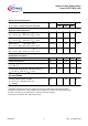
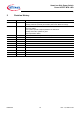
Maximum Ratings at T
j
= 25°C, unless otherwise specified
Parameter
Symbol Value Unit
Drain source voltage V
DS
42 V
Supply voltage for full short circuit protection V
bb
(
SC
)
42
Continuous input voltage
1)
V
IN
-0.2
2)
... +10
Continuous input current
2)
-0.2V £ V
IN
£ 10V
V
IN
< -0.2V or V
IN
> 10V
I
IN
self limited
| I
IN
| £ 2
mA
Operating temperature T
j
-40 ...+150
°C
Storage temperature T
st
g
-55 ... +150
Power dissipation
5)
T
C
= 85 °C
6cm
2
cooling area , T
A
= 85 °C
P
tot
59
1.1
W
Unclamped single pulse inductive energy
2)
E
A
S
3.5
J
Load dump protection V
LoadDump
2)3)
= V
A
+ V
S
V
IN
= 0 and 10 V, t
d
= 400 ms, R
I
= 2 W,
R
L
= 3 W, V
A
= 13.5 V
V
LD
67.5 V
V
ESD
2 kV
Thermal resistance
junction - case: R
thJC
1.1 K/W
SMD: junction - ambient
@ min. footprint
@ 6 cm
2
cooling area
4)
R
thJA
115
55
1
For input voltages beyond these limits I
IN
has to be limited.
2
not subject to production test, specified by design
3
V
Loaddump
is setup without the DUT connected to the generator per ISO 7637-1 and DIN 40839
4
Device on 50mm*50mm*1.5mm epoxy PCB FR4 with 6cm
2 (one layer, 70µm thick) copper area for drain
connection. PCB mounted vertical without blown air.
5
not subject to production test, calculated by R
thJA
and R
ds(on)
Electrostatic discharge voltage
2)
(Human Body Model)
according to Jedec norm
EIA/JESD22-A114-B, Section 4