
Datasheet

BSP129
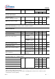
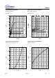
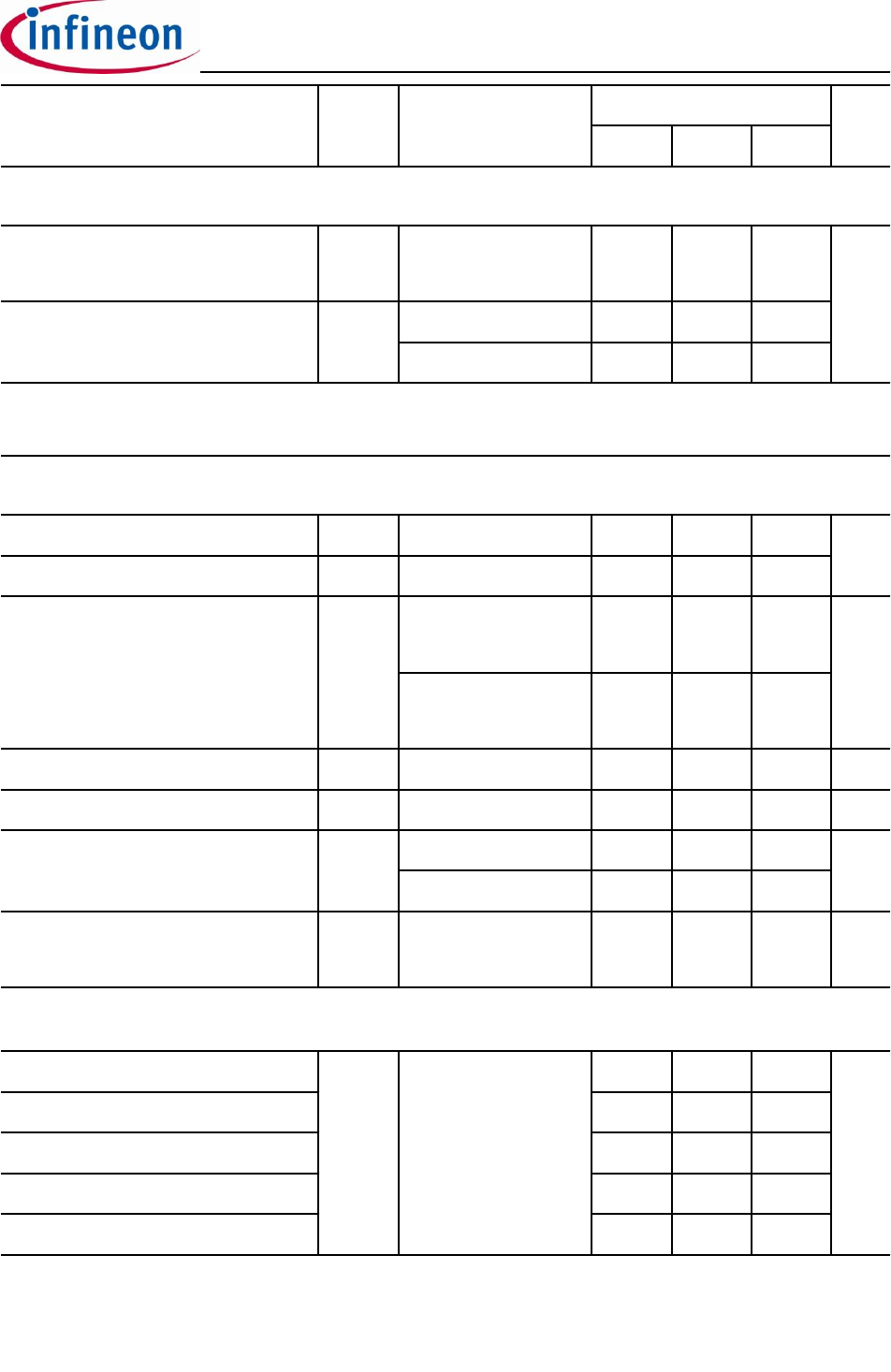
Parameter Symbol Conditions Unit
min. typ. max.
Thermal characteristics
Thermal resistance,
junction - soldering point (pin 4)
R
thJS
- - 25 K/W
SMD version, device on PCB
R
thJA
minimal footprint - - 115
6 cm
2
cooling area
1)
- - 70
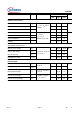
Electrical characteristics, at T
j
=25 °C, unless otherwise specified
Static characteristics
Drain-source breakdown voltage
V
(BR)DSS
V
GS
=-3 V, I
D
=250 µA
240 - - V
Gate threshold voltage
V
GS(th)
V
DS
=3 V, I
D
=108 µA
-2.1 -1.4 -1
Drain-source cutoff current
I
D(off)
V
DS
=240 V,
V
GS
=-3 V, T
j
=25 °C
- - 0.1 µA
V
DS
=240 V,
V
GS
=-3 V, T
j
=125 °C
- - 10
Gate-source leakage current
I
GSS
V
GS
=20 V, V
DS
=0 V
- - 10 nA
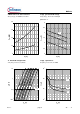
On-state drain current
I
DSS
V
GS
=0 V, V
DS
=10 V
50 - - mA
Drain-source on-state resistance
R
DS(on)
V
GS
=0 V, I
D
=25 mA
- 6.5 20
W
V
GS
=10 V, I
D
=0.35 A
- 4.2 6.0
Transconductance
g
fs
|V
DS
|>2|I
D
|R
DS(on)max
,
I
D
=0.28 A
0.18 0.36 - S
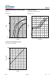
Threshold voltage V
GS(th)
sorted in bands
3)
J
V
GS(th)
V
DS
=3 V, I
D
=108 µA
-1.2 - -1 V
K -1.35 - -1.15
L -1.5 - -1.3
M -1.65 - -1.45
N -1.8 - -1.6
drain connection. PCB is vertical in still air.
3)
Each reel contains transistors out of one band whose identifying letter is printed on the reel label. A specific
band cannot be ordered separately.
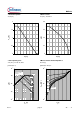
Values
2)
Device on 40 mm x 40 mm x 1.5 mm epoxy PCB FR4 with 6 cm
2
(single layer, 70 µm thick) copper area for
Rev. 1.41
page 2
2012-03-20