
Datasheet


= =
=
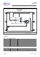
Source 1 Source 2
Source 3
5V=
S 4
S 7
S 1
R 1
R 2
S 8
S 9
S 6
S 2
S 3
AC Measurement
BCR450_Test circuit.vsd
Source 4
S 5
Source 5
PWM
=
Vref
V
s
V
sense
I
Out
EN
GND
+
-
=
~ 150 mV
Vout
Datasheet 6 Rev. 3.1, 2013-02-21
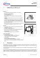
BCR450
LED Driver IC
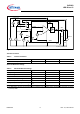
Description
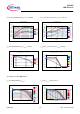
Figure 2 Electrical test circuit
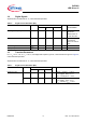
Thermal resistance
Table 3 Thermal resistance
Parameter Symbol Value Unit
Junction - solder point
R
thJS
75 K/W
Absolute Maximum Ratings
Table 4 Absolute Maximum ratings
Parameter Symbol Limit Value Unit
Supply voltage
V
s
40 V
Sense Voltage
Vsense 200 mV
Output current I
out 100 mA
Total Power Dissipation; T
s
= 112.5°C P
tot
500 mW
Junction temperature
T
J
150 °C
Storage temperature range
T
STG
-65... 150 °C
ESD capability Human Body Model
1)
1) For ESD testing, the chip was mounted in a SC74 package on an application board, where GND is electrically connected
to the chip GND
V
ESD_HBM
2000 V