
Datasheet
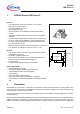
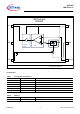
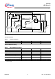
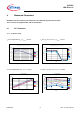

BCR450_Block diagram.vsd
6
5
43
2
1Iout
GND
EN
Vs
GND
Vsense
LED Controller
BCR450
Vref
OP
Output
stage
Bandgap
BCR450
LED Driver IC
Description
Datasheet 5 Rev. 3.1, 2013-02-21
Figure 1 Block diagram
Pin Definition
Table 1 Pin definition and function
Pin number Pin Symbol Function
1
I
out
Controlled output current to drive LEDs
2 GND IC ground
3 EN Power On control voltage pin (PWM inpu
t)
4
V
sense
Sense control voltage pin for internal feedback mechanism
5 GND IC ground
6
V
s
Supply voltage
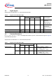
Table 2Marking
Type Marking Package
BCR450 50s SC74