
Datasheet

BCR401U
Electrical Characteristics
Datasheet 9 Revision 2.0, 2012-04-12
2 Electrical Characteristics
Attention: Stresses above the max. values listed here may cause permanent damage to the device.
Exposure to absolute maximum rating conditions for extended periods may affect device
reliability. Maximum ratings are absolute ratings; exceeding only one of these values may
cause irreversible damage to the integrated circuit.
Table 2-1 Maximum Ratings at
T
A
= 25 °C, unless otherwise specified
Parameter Symbol Values Unit Note / Test Condition
Min. Typ. Max.
Supply voltage
V
S
--40V
Output current
I
out
--65mA
Output voltage
V
out
--40V
Reverse voltage between all terminals
V
R
--0.5V
Total power dissipation
P
tot
--750mWT
S
≤ 112.5 °C
Junction temperature
T
J
--150°C
Storage temperature range
T
STG
-65 - 150 °C
Table 2-2 Thermal Resistance at
T
A
= 25 °C, unless otherwise specified
Parameter Symbol Values Unit Note / Test Condition
Min. Typ. Max.
Junction - soldering point
1)
1) For calculation of R
thJA
please refer to Application Note AN077 (Thermal Resistance Calculation)
R
thJS
--50K/W
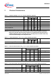
Table 2-3 Electrical Characteristics at
T
A
= 25 °C, unless otherwise specified
Parameter Symbol Values Unit Note / Test Condition
Min. Typ. Max.
Collector-emitter breakdown voltage
V
BR(CEO)
40 - - V I
C
=1mA, I
B
=0
Supply current
I
S
340 420 500 µA V
S
=10V
DC current gain
h
FE
100 220 470 - I
C
=50mA, V
CE
=1V
Internal resistor
R
int
78 91 104 Ω I
Rint
=10mA
Output current
I
out
91011mAV
S
=10V
V
out
=8.6V
Voltage drop (
V
Rext
) V
drop
0.82 0.91 1 V I
out
=10mA
Table 2-4 DC Characteristics with stabilized LED load at
T
A
= 25 °C, unless otherwise specified
Parameter Symbol Values Unit Note / Test Condition
Min. Typ. Max.
Lowest sufficient supply voltage overhead
V
Smin
-1.4-VI
out
>18mA
Output current change versus
T
A
∆I
out
/I
out
--0.2-%/KV
S
=10V
Output current change versus
V
S
∆I
out
/I
out
-1-%/VV
S
=10V