
Datasheet


BCR320U / BCR321U
Electrical Characteristics
Datasheet 9 Revision 2.0, 2012-05-04
2 Electrical Characteristics
Attention: Stresses above the max. values listed here may cause permanent damage to the device.
Exposure to absolute maximum rating conditions for extended periods may affect device
reliability. Maximum ratings are absolute ratings; exceeding only one of these values may
cause irreversible damage to the integrated circuit.
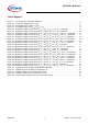
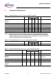
Table 2-1 Maximum Ratings at
T
A
= 25 °C, unless otherwise specified
Parameter Symbol Values Unit Note / Test Condition
Min. Typ. Max.
Enable voltage
BCR320U
BCR321U
V
EN
-
-
-
-
25
4.5
V
Output current
I
out
--300mA
Output voltage
V
out
--16V
Reverse voltage between all terminals
V
R
--0.5V
Total power dissipation
P
tot
- - 1000 mW T
S
≤ 100 °C
Junction temperature
T
J
--150°C
Storage temperature range
T
STG
-65 - 150 °C
Table 2-2 Thermal Resistance at
T
A
= 25 °C, unless otherwise specified
Parameter Symbol Values Unit Note / Test Condition
Min. Typ. Max.
Junction - soldering point
1)
1) For calculation of R
thJA
please refer to Application Note AN077 (Thermal Resistance Calculation)
R
thJS
--50K/W
Table 2-3 Electrical Characteristics at T
A
= 25 °C, unless otherwise specified
Parameter Symbol Values Unit Note / Test Condition
Min. Typ. Max.
Collector-emitter breakdown voltage
V
BR(CEO)
16 - - V I
C
=1mA, I
B
=0
Enable current
BCR320U
BCR321U
I
EN
-
-
1.2
1.2
-
-
mA
V
EN
=12V
V
EN
=3.3V
DC current gain
h
FE
200 350 500 - I
C
=50mA, V
CE
=1V
Internal resistor
R
int
85 95 105 Ω I
Rint
=10mA
Bias resistor
BCR320U
BCR321U
R
B
-
-
10
1.5
-
-
kΩ