
Datasheet


Application Note No. 058
Predicting Distortion in PIN-Diode Switches
Application Note 9 Rev. 2.1, 2006-10-20
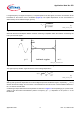
Figure 14 Formula 10
Figure 15 Formula 11
Here τ
L
and r
f
denote the effective lifetime and resistance available from the diode data sheet. R
s
denotes the
series resistance of highly doped p
++
and n
++
regions as well as the package resistance. With the typical value of
R
s
= 0.2 Ω, P
max
can be estimated from PIN-diode data sheet parameters.
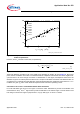
In Figure 12 measurement results for a variety of PIN-diodes at different operation currents are compared to
results of our simple model. The comparison shows that third-order inter-modulation for P
0
< P
max
can be well
predicted with (10) from the diode data sheet parameters.
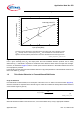
Figure 16 shows third-order inter-modulation for the PIN-diode BAR65-03W at different bias currents. Our model
shows good agreement with measurement results. For an input power higher than P
max
intermodulation increases
more rapidly than predicted with our model.
AN058_formula_10.vs
d
(10)
2/3
2
0
2
23
−
=
sf
L
T
Rr
If
ZvIP
τπ
AN058_formula_11.vs
d
(11)
2
0max
2
2
1
−
=
sf
L
T
Rr
If
vZP
τπ