
Datasheet


Application Note 8 Rev. 2.1, 2006-10-20
Application Note No. 058
Predicting Distortion in PIN-Diode Switches
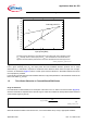
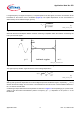
Figure 12 Comparison of IP
3
measurement results with calculation results based on PIN-diode
datasheet parameters
However, when P
0
exceeds a certain limit, as specified by
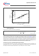
Figure 13 Formula (9)
Third-order distortion increases much more rapidly than described by relation (6) (see Figure 3). Above this
power, the AC-modulation of the carrier concentration leads to a depletion of the intrinsic zone in the negative half-
cycle and thus to an even stronger non-linear i-v-characteristic. In this region, assumptions which led to the
derivation of (6) are not valid anymore and thus the
IP
3
concept for calculation of the third-order distortion fails. As
a consequence, to suppress third-order distortion, the diode should always be operated in regions where
P
0
< P
max
is fulfilled. For given P
0
and a certain diode this requires at least a minimum operating current.
Calculation of IP
3
and P
max
from PIN-Diode Data Sheet Parameters
For most PIN-diodes the current in the region of interest is rather determined by surface recombination and
recombination in the p
++
and n
++
regions than by bulk recombination in the intrinsic region. Thus the electron and
hole charge in the intrinsic region is proportional to τ sqrt (I). With (3) for
IP
3
and P
max
follows:
AN058_IP3_measurement.vsd
0.1 1 10 100
40
60
80
100
Ba592
Bar63
Bar65
Ba597
Ba595
Bar64
Bar66
Bar14
IP3 [dBm]
I
τ
L
ω
/ (r
f
-R
s
) [A
2
/V]
AN058_formula_9.vs
d
(9)
2
2
2
0max
2
τ
π
f
W
D
IZP
=