
Datasheet


Application Note 12 Rev. 2.1, 2006-10-20
Application Note No. 058
References
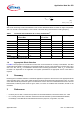
Nomenclature
V
out
Output voltage
V
in
Input voltage
A
1
, A
2
, A
3
Taylor coefficients of device transfer characteristics
f
1
, f
2
Input frequencies
r
F
High-frequency resistance of the PIN-diode intrinsic region
µ
n
, µ
p
Electron and hole mobility
W Intrinsic region thickness
τ Carrier lifetime in the intrinsic region
D Ambipolar diffusion-coefficient
f Frequency
L
AC
AC difussion-length
V
T
Thermal-voltage
P
IM3
Third-order inter-modulation power
IP
3
Intercept point power
P
0
Power of fundamental frequency
Z
0
Characterictic (wave) impedance
P
max,IP3
Power limit for the validity of the IP3-concept
R
S
PIN-diode series resistance
τ
L
PIN-diode recovery time available from the data sheet
C
d
PIN-diode small signal depletion capacitance
V
R
Reverse voltage
P
max,rev.
Maximum power in reverse mode for prevention of intermodulation increase