
Datasheet


Application Note 10 Rev. 2.1, 2006-10-20
Application Note No. 058
Predicting Distortion in PIN-Diode Switches
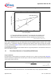
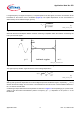
Figure 16 Third-order inter-modulation
1.3 Distortion in Reverse-Biased PIN-Diodes
The RF-characteristics of the reverse biased PIN-diode is primarily determined by the (small signal) depletion
capacitance
C
d
. Thie capacitance generally depends only slightly on the reverse-voltage. These variations give
rise to another generation of intermodulation products. For a diode switch within this simple model the intercept
point for the third-order intermodulation poduct is given by (2)
Figure 17 Formula 12
The voltage-dependence of the capacitance is due to the variation of the depletion region with increasing reverse-
bias and therefore mainly determind by the diffusion tails of the highly doped p
++
and n
++
contact regions of the
PIN-diode. Since this dependence decreases with the width of the intrinsic region, inter-modulation is weaker for
thicker PIN-diodes.
If the diode gets forward biased during the half-wave of the RF-signal, carrier injection into the intrinsic region
significantly reduces the width of the depletion region. Thus for power-levels higher than [
Formula 13] diodes with
small intrinsic region might show a major increase of inter-modulation.
AN058_IP3_third_order_inter_modulation.v
s
10 15 20 25 30 35
-100
-80
-60
-40
-20
0
20
40
10
5
2
1
P
max
P
0
I [mA]
0.3
Bar65-03w
f = 900 MHz
P
IM3
[dBm]
Pin [dBm]
Third-order inter-modulation for PIN-diode BAR65-03W at differend current levels and RF-
input power for a 50 Ω antenna switch compared to calucations of equation (10), (8) (solid).
Also shown are the validity limits P
max
(11) for the IP
3
concept
AN058_formula_12.vs
d
(12)
1
2
0
2
2
)2(
d
d
32
1
3
−
= fZ
V
C
IP
R
d
π