A pp li c a t i o n N o t e , R e v . 2 . 1 , O c t . 2 00 6 A p p li c a t i o n N o t e N o .
Edition 2006-10-20 Published by Infineon Technologies AG 81726 München, Germany © Infineon Technologies AG 2009. All Rights Reserved. Legal Disclaimer The information given in this document shall in no event be regarded as a guarantee of conditions or characteristics (“Beschaffenheitsgarantie”).
Application Note No. 058 Application Note No. 058 Revision History: 2006-10-20, Rev. 2.1 Previous Version: Edition A02 Page Subjects (major changes since last revision) All Document layout change Application Note 3 Rev. 2.
Application Note No. 058 Predicting Distortion in PIN-Diode Switches 1 Predicting Distortion in PIN-Diode Switches This application note describes the orgin of distortion in PIN-diode switches. Distrotion is related to physical parameters of the diode and operating conditions and thus can be minimized by an appropriate diode selection.
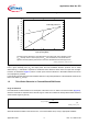
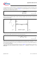
Application Note No. 058 Predicting Distortion in PIN-Diode Switches 70 60 output power [dBm] 50 intercept point IP3 40 30 20 P 10 0 0 -10 -20 P -30 P -40 max IM3 -50 -60 -70 0 10 20 30 40 input power [dBm] Theoretical power dependence of fundamental (P 0) and third-order inter modulation product (PIM3). Actually, above a certain input power Pmax , inter-modulation of a PIN-diode shows a significant increase (dashed) and therefore cannot be calculated from the intercept point IP 3.
Application Note No. 058 Predicting Distortion in PIN-Diode Switches If a high-frequency AC-signal of frequency f is superimposed to the DC signal, the carrier concentration at the boundaries of the intrinsic zone is modulated (Figure 6). The spatial dependence of this concentration is determined by the AC-diffusion length, given by LAC = Dτ 1 + j ( 2πfτ ) (4) AN058_formula_4.vsd Figure 5 Formula (4) Where D denotes the ambipolar diffusion constant.
Application Note No. 058 Predicting Distortion in PIN-Diode Switches 2 PIM 3 3 vT = 4 Z04 6 3 W P0 I τ 2πf1 D (6) AN058_formula_6.vsd Figure 8 Formula (6) Where rf << Z0 has been assumed. This gives for the intercept-point IP3 = 4 1 2 2π I D τ f Z0 3 vT W2 3/ 2 (7) AN058_formula_7.
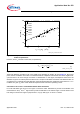
Application Note No. 058 Predicting Distortion in PIN-Diode Switches 100 Ba592 Bar63 Bar65 80 Ba597 IP3 [dBm] Ba595 Bar64 Bar66 60 Bar14 40 0.1 1 10 I τ ω / (r -R ) L f s 100 [A2/V] AN058_IP3_measurement.vsd Figure 12 Comparison of IP3 measurement results with calculation results based on PIN-diode datasheet parameters However, when P0 exceeds a certain limit, as specified by Pmax π 2 D = Z0 I f τ 2 2 W 2 (9) AN058_formula_9.
Application Note No. 058 Predicting Distortion in PIN-Diode Switches 2π f τ L I IP3 = 2vT Z 0 rf − Rs 3/ 2 2 (10) A N058_formula_10.vsd Figure 14 Formula 10 Pmax 2π f τ L I 1 = Z 0 vT r −R 2 s f 2 (11) A N058_formula_11.vsd Figure 15 Formula 11 Here τLand rf denote the effective lifetime and resistance available from the diode data sheet. Rs denotes the series resistance of highly doped p++ and n++ regions as well as the package resistance.
Application Note No. 058 Predicting Distortion in PIN-Diode Switches 40 P 20 0 0 P -40 P IM3 [dBm] max -20 -60 -80 I [mA] 0.3 1 2 Bar65-03w 5 -100 10 f = 900 MHz 10 15 20 25 30 35 Pin [dBm] Third-order inter-modulation for PIN-diode BAR65-03W at differend current levels and RFinput power for a 50 Ω antenna switch compared to calucations of equation (10), (8) (solid). Also shown are the validity limits Pmax (11) for the IP3 concept AN058_IP3_third_order_inter_modulation.
Application Note No. 058 Summary 2 Pmax,rev. V = R 2Z 0 (13) A N058_formula_13.vsd Figure 18 Formula 13 Also worth mentioning is that intermodulation of the reverse biased PIN-diode increases for higher frequencies. This is in contrast to intermodulation in the on-state of the diode being reduced with increasing frequency.
Application Note No. 058 References Nomenclature Vout Vin A1, A2, A3 f1, f2 rF Output voltage µn, µp Electron and hole mobility W Intrinsic region thickness τ Carrier lifetime in the intrinsic region D f LAC VT PIM3 IP3 P0 Z0 Pmax,IP3 RS Ambipolar diffusion-coefficient τL PIN-diode recovery time available from the data sheet Cd VR Pmax,rev.