
Datasheet


AUIR3313(S)
www.irf.com
4
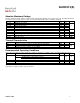
Protection Characteristics
Tj=-40°..150°C, Vcc=6..26V, Rifb=300 to 5k
Symbol
Parameter
Min.
Typ.
Max.
Units
Test Conditions
Vifb-Vin@Isd
Over-current shutdown threshold
3.8
4.7
5.9
V
Tsd
Over temperature threshold
165
°C
See fig. 5
OV
Over voltage protection (not latched)
33
35
39
V
Isdf
Fixed over current shutdown
90
120
150
A
Vifb<Vifb-Vin@Isd
Isd_1k
Programmable over current shutdown 1k
30
40
53
Rifb=1k
treset
Time to reset protection
50
500
µs
See fig. 5
Min. pulse
Min. pulse width (no WAIT state)
150
400
1200
Tj=25°C
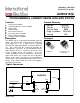
WAIT
WAIT function timer
0.4
1
2
ms
See fig. 4 and 5
Rds(on) rev.
Reverse battery On state resistance
Tj=25°C
4
6.7
10
m
Vcc-Vin=-14V,
Iout=30A
Tj=125°C
10
15
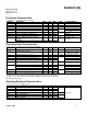
Static Electrical Characteristics
Tj=-40°..150°C, Vcc=6..26V (unless otherwise specified)
Symbol
Parameter
Min.
Typ.
Max.
Units
Test Conditions
Vcc op.
Operating Voltage range
6
32
V
Icc off
Supply leakage current
1.5
5
µA
Vin=Vcc, Vcc-Vout=14V,
Vcc-Vifb=14V, Tj=25°C
Iin, on
On state IN positive current
1.5
3
6
mA
Vcc-Vin=14V, Tj=25°C
Vih
High level Input threshold voltage (4)
5.4
6.3
V
Vil
Low level Input threshold voltage (4)
4
4.9
5.8
Vhyst
Input hysteresis Vih-Vil
0.2
0.4
1.5
Iout
Drain to source leakage current
1.2
5
µA
Vin=Vcc, Vcc-Vifb=0V,
Vcc-Vout=14V, Tj=25°C
Rds(on)
On state resistance (5) Tj=25°C
5.5
7
m
Iout=30A, Vcc-Vin=14V
On state resistance (5) Tj=25°C
6
10
Iout=17A, Vcc-Vin=6V
On state resistance (5)(6) Tj=150°C
10.5
13.5
Iout=30A, Vcc-Vin=14V
V clamp1
Vcc to Vout clamp voltage 1
36
39
V
Iout=50mA
V clamp2
Vcc to Vout clamp voltage 2
40
43
Iout=30A, Tj=25°C
(4) Input thresholds are measured directly between the input pin and the tab. Any parasitic resistance in common between
the load current path and the input signal path can significantly affect the thresholds.
(5) Rdson is measured between the tab and the Out pin, 5mm away from the package.
(6) Guaranteed by design
Switching Electrical Characteristics
Vcc=14V, Resistive load=0.5 , Tj=25°C
Symbol
Parameter
Min.
Typ.
Max.
Units
Test Conditions
tdon
Turn on delay time to 10% Vcc
8
32
80
µs
See figure 2
tr1
Rise time to Vcc-Vout=5V
3
16
40
tr2
Rise time to Vcc-Vout=0.1Vcc
6
40
90
Eon
Turn on energy
4.5
mJ
tdoff
Turn off delay time
20
80
200
µs
tf
Fall time to Vout=10% of Vcc
8
32
80
Eoff
Turn off energy
2
mJ