
Datasheet


AUIPS6031(S)(R)
www.irf.com
7
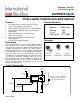
Vds
Ids
Vin
Vcc
Vds clamp
T clamp
See Application Notes to evaluate power dissipation
Tj
Ilim
Tsd+
Tsd-
Iout
Vin
limiting
Thermal cycling
DG
Figure 1 – Active clamp waveforms
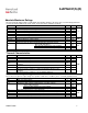
Figure 2 – Protection timing diagram
Vout
Vin
Tr-in
90%
10%
90%
10%
Td on
Tr1
Td off
Tf
Vcc-5V
Tr2
Vcc
Figure 3 – Switching times definitions
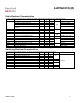
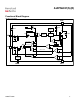
Figure 4 – Active clamp test circuit
Vclamp
Iout
Vin
In
Vcc
Out
R
L
0V
5V
14V
+
-
Vout
Rem :
During active
clamp, Vload
is negative
Dg
Gnd