
User Manual


POC-17i/19i Series
Page 22
Figure 3-3: Clear CMOS Jumper
3.6.4 COM1 Pin 9 Setting
Jumper Label:
JP7 and JP8
Jumper Type:
6-pin header
Jumper Settings:
See
Table 3-4 and Table 3-5
Jumper Location:
See
Figure 3-4 and Figure 3-5
Two jumpers (JP7 and JP8) configure pin 9 on COM1 and COM3 DB-9 connectors. Pin 9
on the COM1 and the COM3 DB-9 connectors can be set as the ring (RI) signal, +5 V or
+12 V. The COM1 and COM3 Pin 9 Setting jumper selection options are shown in the
tables below.
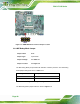
JP7 Description
Short 1-2 COM1 RI +12 V
Short 3-4 COM1 RI Normal
Short 5-6 COM1 RI Pin +5 V
Table 3-4: COM1 Pin 9 Setting Jumper Settings