
Instruction Manual
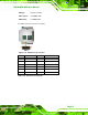


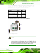
Table Of Contents
- 1 Introduction
- 2 Unpacking
- 3 Connectors
- 3.1 Peripheral Interface Connectors
- 3.2 Internal Peripheral Connectors
- 3.2.1 12V / 5V Power Connector
- 3.2.2 ATX Power Supply Enable Connector
- 3.2.3 Audio Kit Connector
- 3.2.4 Battery Connector
- 3.2.5 CompactFlash® Connector
- 3.2.6 Fan Connector
- 3.2.7 Digital I/O Connector
- 3.2.8 Keyboard/Mouse Connector
- 3.2.9 LAN Connector
- 3.2.10 LCD Inverter Connector
- 3.2.11 LED and +5V Output Connector
- 3.2.12 PCI-104 Connector
- 3.2.13 Power Button Connector
- 3.2.14 Reset Button Connector
- 3.2.15 RS-232 Serial Port Connectors
- 3.2.16 RS-422/485 Serial Port Connector
- 3.2.17 LVDS LCD Connector
- 3.2.18 SATA Drive Connector
- 3.2.19 SPI Flash Connector
- 3.2.20 USB Connector
- 3.2.21 VGA Connector
- 4 Installation
- 5 BIOS
- A BIOS Options
- B Terminology
- C Watchdog Timer
- D Hazardous Materials Disclosure
PM-945GSE-N270 User Manual
Page 60
Setting DESCRIPTION
1-2 RS-232 (Default)
3-4 RS-422
5-6 RS-485
7-8 RS-485 with RTS# control
Table 4-2: COM3 RS-232/422/RS485 Select Jumper Settings
Figure 4-4: COM3 RS-232/422/RS485 Select Jumper Location
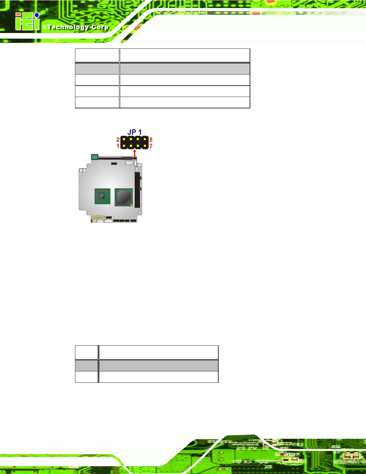
4.5.3 LVDS Voltage Select Jumper
Jumper Label:
J_LVDS1
Jumper Type:
3-pin header
Jumper Location:
See Figure 4-2
Jumper Setti
ngs:
See Table 4-3
The LVDS V
oltage Select jumper sets the LVDS voltage to +3.3V or +5V.
JP1 DESCRIPTION
1-2 LCD/VCC +3.3V (Default)
2-3 LCD/VCC +5V
Table 4-3: LVDS Voltage Select Jumper Settings