
Manual


Table Of Contents
- 1 Introduction
- 2 Packing List
- 3 Connector Pinouts
- 3.1 Peripheral Interface Connectors
- 3.2 Internal Peripheral Connectors
- 3.2.1 ATX Power Signal Connector
- 3.2.2 Battery Connector
- 3.2.3 Digital I/O Connector
- 3.2.4 DisplayPort Connector
- 3.2.5 EC Debug Port
- 3.2.6 Fan Connector (CPU)
- 3.2.7 Fan Connector (System)
- 3.2.8 Front Panel Connector
- 3.2.9 Keyboard/Mouse Connector
- 3.2.10 LAN Active LED Connector
- 3.2.11 LVDS Connector
- 3.2.12 LVDS Backlight Connector
- 3.2.13 PCIe Mini Card Slot (Full-size)
- 3.2.14 PCIe Mini Card Slot (Half-size)
- 3.2.15 PCI Express x16 Slot
- 3.2.16 Power Button (On-board)
- 3.2.17 Power Connector (12V)
- 3.2.18 RS-232 Serial Port Connectors (COM2 ~ COM5)
- 3.2.19 RS-422/485 Serial Port Connector (COM6)
- 3.2.20 SATA 6Gb/s Drive Connectors
- 3.2.21 SATA 3Gb/s Drive Connectors
- 3.2.22 SATA Power Connectors
- 3.2.23 SMBus Connector
- 3.2.24 SO-DIMM Connectors
- 3.2.25 SPI Flash Connector
- 3.2.26 SPI Flash Connector (EC)
- 3.2.27 TPM Connector
- 3.2.28 USB 2.0 Connectors
- 3.2.29 USB 3.0/2.0 Connector
- 3.3 External Interface Connectors
- 4 Installation
- 4.1 Anti-static Precautions
- 4.2 Installation Considerations
- 4.3 Cooling Kit Installation
- 4.4 SO-DIMM Installation
- 4.5 PCIe Mini Card Installation
- 4.6 Jumper Settings
- 4.7 Chassis Installation
- 4.8 Internal Peripheral Device Connections
- 4.9 External Peripheral Interface Connection
- 4.10 Intel® AMT Setup Procedure
- 5 BIOS
- 5.1 Introduction
- 5.2 Main
- 5.3 Advanced
- 5.3.1 ACPI Settings
- 5.3.2 RTC Wake Settings
- 5.3.3 Trusted Computing
- 5.3.4 CPU Configuration
- 5.3.5 SATA Configuration
- 5.3.6 Intel(R) Rapid Start Technology
- 5.3.7 AMT Configuration
- 5.3.8 USB Configuration
- 5.3.9 iWDD H/W Monitor
- 5.3.10 F81866 Super IO Configuration
- 5.3.11 F81866 H/W Monitor
- 5.3.12 Serial Port Console Redirection
- 5.3.13 iEi Feature
- 5.4 Chipset
- 5.5 Boot
- 5.6 Security
- 5.7 Save & Exit
- 6 Software Drivers
- A BIOS Options
- B One Key Recovery
- C Terminology
- D Digital I/O Interface
- E Hazardous Materials Disclosure
KINO-DQM871 Mini-ITX SBC
Page 65
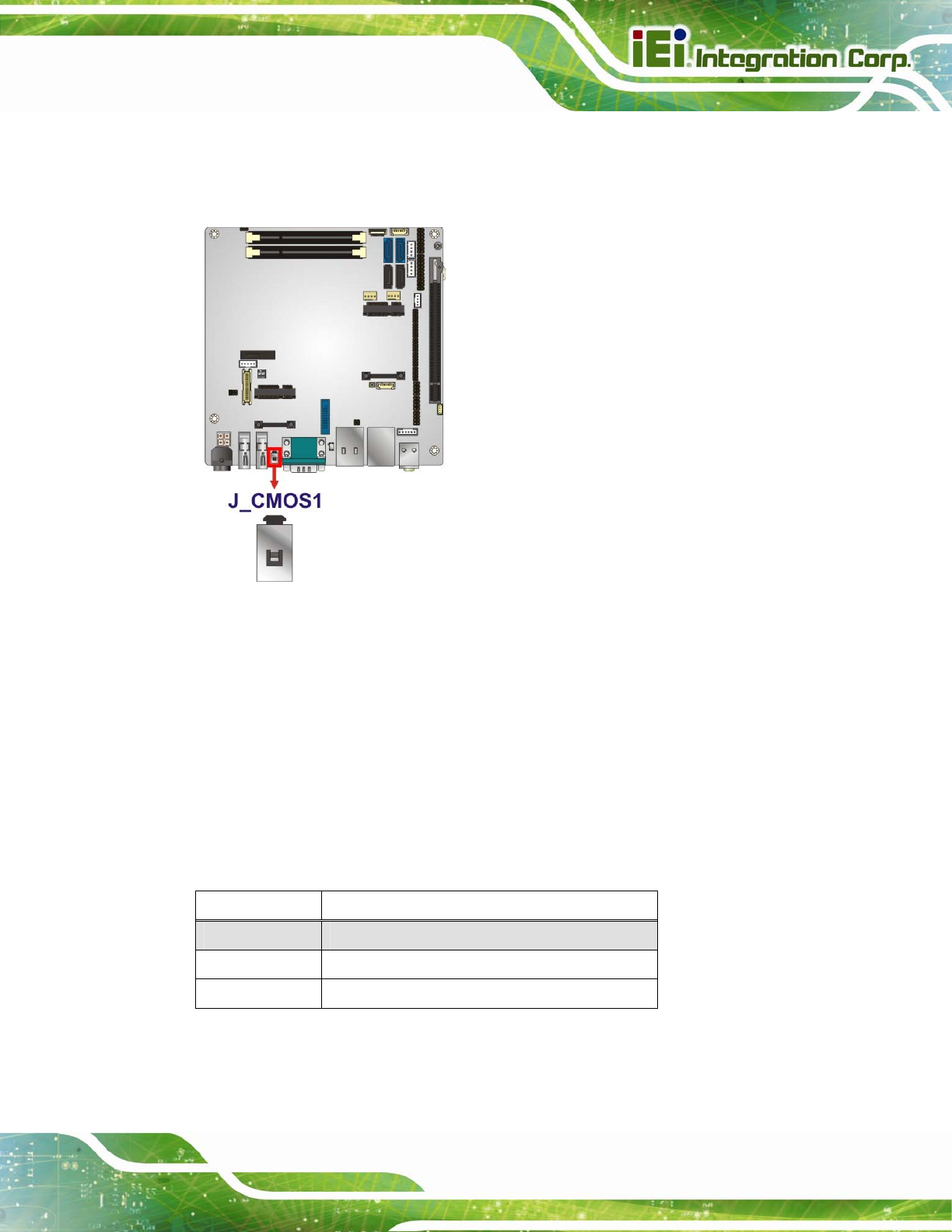
Load Failsafe Defaults.
After having done one of the above, save the changes and exit the CMOS Setup menu.
Figure 4-7: Clear CMOS Jumper Location
4.6.3 LVDS Voltage Selection
Jumper Label: JLCD_PWR1
Jumper Type:
6-pin header
Jumper Settings:
See
Table 4-2
Jumper Location:
See
Figure 4-8
This jumper selects the voltage of the LVDS connector.
Pin Description
Short 1-2 +3.3 V (Default)
Short 3-4 +5 V
Short 5-6 +12 V
Table 4-2: LVDS Voltage Selection Jumper Settings