
Manual
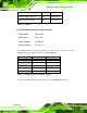
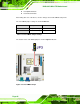
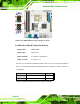
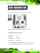
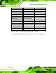
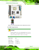

Table Of Contents
- 1 Introduction
- 2 Detailed Specifications
- 3 Unpacking
- 4 Connector Pinouts
- 4.1 Peripheral Interface Connectors
- 4.2 Internal Peripheral Connectors
- 4.2.1 Fan Connectors
- 4.2.2 Front Panel Connector
- 4.2.3 Digital Input/Output Connector
- 4.2.4 IDE Connector
- 4.2.5 LCD Backlight Connector
- 4.2.6 LVDS LCD connector
- 4.2.7 Power Connector
- 4.2.8 14-Pin Serial Port Connectors
- 4.2.9 10-Pin Serial Port Connectors
- 4.2.10 SATA Drive Connectors
- 4.2.11 SPDIF Connector
- 4.2.12 Internal USB Connectors
- 4.3 External Interface Connectors
- 5 Installation
- 6 AMI BIOS
- 7 Driver Installation
- A BIOS Options
- B DIO Interface
- C Watchdog Timer
KINO-9453 Mini-ITX Motherboard
Page 69
JP9 Description
Open Normal Operation Default
Short Termination Resister Setting
Table 5-6: RS-485 Termination Resister Jumper Settings
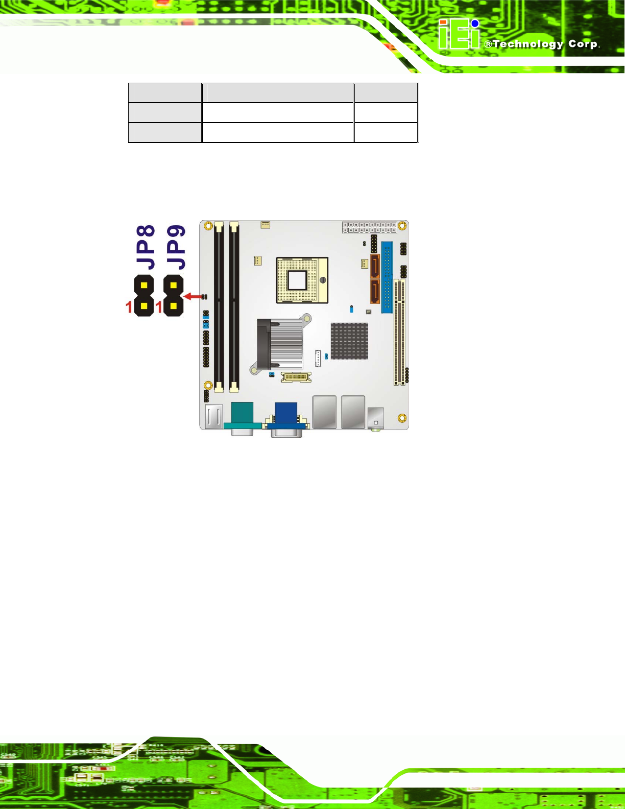
The RS-422 or RS-485 Termination Resister jumper location is shown in Figure 5-11.
Figure 5-11: RS-422 and RS-485 Termination Resister Jumper Locations
5.4.5 LVDS Screen Resolution Selection
Jumper Label: JP2
Jumper Type:
8-pin header
Jumper Settings: See
Table 5-8
Jumper Location: See
Figure 5-13
The LVDS Screen Resolution Selection jumper allows the LVDS screen resolution to be
set. The LVDS Screen Resolution Selection jumper settings are shown in
Table 5-8.